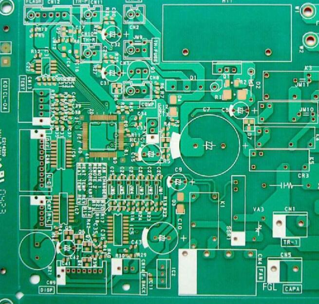
The basic electrical function of a printed circuit is to supply electrical energy to each electronic component and to transmit electrical signals from one electronic component to another electronic component (such as a transistor or an integrated circuit). работа с быстрым переключением транзисторов, the transistor needs to be turned on or cut off a large current instantaneously, колебание напряжения питания, Устойчивое функционирование оборудования. When working at low speed, only a simple electrical connection is required between the signal sending end (device) and the signal receiving end (device). Однако, when working at high speeds, the connection line (microstrip line) is required to have a special shape and length, as well as a special arrangement of power planes and ground planes, При такой передаче сигнала не будет серьезных искажений формы. если не предусмотрено иное, the waveform of the signal transmitted from one end to the other must not be significantly altered. Слишком длинная линия передачи не подходит для передачи высокоскоростных сигналов, because in the process of high-speed pulse transmission, предварительный импульс может не дойти до конца приёмника, but the secondary pulse has left the transmitting end. повышение частоты, Чем скорее сигнал, тем больше вероятность интерференции и электромагнитных помех, and the more difficult it will be to prevent the circuit from being subjected to signal intermodulation interference or electromagnetic interference. для стабилизации питания, many decoupling capacitors are required between the power supply layer and the ground layer. рациональное проектирование схемы проводника, слоистая конструкция и линии передачи сигналов могут снизить шум. In a multilayer PCB, поверхность питания должна быть близко к кристаллу, чтобы снизить сопротивление питания. The structure of the power supply surface close to the wiring layer can effectively reduce the radiation noise.

второй, the printed circuit designer should first read the circuit schematic
If the designer of a printed circuit wants to design a circuit schematic into a qualified printed circuit, Он должен сначала понять схему. The so-called understanding is not a designer who is demanding a printed circuit board, как и конструктор - конструктор, especially in the case of using computer-aided design (CAD) to design a printed circuit board. основные знания об электронных схемах. и некоторые неясные вопросы в электронных схемах, you can communicate with the designer of the circuit schematic in time.
три стороны, double-sided and multi-layer PCB design procedures are quite different
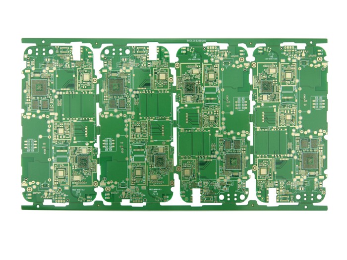
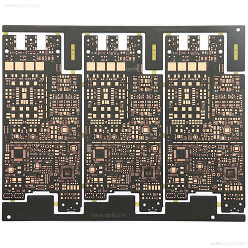
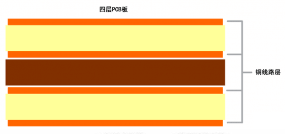
The manufacturing processes of single-sided printed circuit boards, двусторонняя печатная плата и многослойная печатная плата сильно отличаются друг от друга. Simply put, плата для односторонней и двухсторонней печатной схемы, you can first make a copper-clad board, затем дизайн печатных плат, and selectively corrode the conductors (including pads) on the surface of the copper-clad board The graphics are made into a printed circuit board, То есть, the design of the printed circuit board can be before the production of the copper-clad board, После изготовления бронзовых листов. However, многослойная печатная плата должна сначала по дизайну печатных плат производить на поверхности изоляционной плиты внутренний слой с медным цоколем, потом пластифицировать их в печатную схему. целая печатная плата, that is, the design of the multilayer PCB board must be arranged before the printed circuit board is manufactured.