1. определение формы пластины, size and number of layers
Any printed board has the problem of matching with other structural parts. поэтому, the shape and size of the printed board must be based on the structure of the product. Однако, from the perspective of the production process, Это должно быть как можно проще, generally a rectangle with a not too wide aspect ratio to facilitate assembly, повышение эффективности производства, and reduce labor costs.

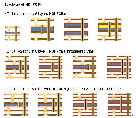
необходимо определить число слоев по требованиям характеристик цепи, board size and circuit density. многослойная печатная плата, four-layer boards and шесть-layer boards are the most widely used. пример с четырёхслойными пластинами, there are two conductor layers (component surface and soldering surface), уровень питания и уровень земли.
The layers of the multi-layer board should be symmetrical, лучше всего иметь четное медное покрытие, То есть, four, six, eight, и так далее. Because of the asymmetrical lamination, поверхность платы легко коробиться, especially for surface-mounted multilayer boards, Это заслуживает большего внимания..
2. The location and orientation of components
The location and placement direction of the components should first be considered from the circuit principle to cater to the direction of the circuit. Разумность укладки непосредственно влияет на качество печатных плат, especially the high-frequency analog circuit, Это делает оборудование более строгим. рациональное размещение компонентов, in a sense, предвещать успех в проектировании печатной доски. Therefore, начать компоновку печатных плат и определить их общую компоновку, a detailed analysis of the circuit principle should be carried out, and the location of special components (such as large-scale ICs, high-power tubes, сигнальный источник, etc.) should be determined first, and then Arrange other components and try to avoid factors that may cause interference.
С другой стороны, it should be considered from the overall structure of the printed board to avoid uneven and disordered arrangement of components. Это не только влияет на красоту печатных плат, but also brings a lot of inconvenience to assembly and maintenance work.
3. Requirements for wiring layer and wiring area
In general, монтаж многослойных печатных плат производится в соответствии с функцией схемы. In the outer layer wiring, для сварки поверхности нужно больше проводов, а поверхности деталей нужно меньше проводов, which is conducive to the maintenance and troubleshooting of the printed board. разреженный, dense wires and signal wires that are susceptible to interference are usually arranged in the inner layer. большая медная фольга должна равномерно распространяться внутри и снаружи, which will help reduce the warpage of the board and also make the surface more uniform during electroplating. для предотвращения формования обработки в процессе механической обработки повредить печатные линии, вызвать межпластовое короткое замыкание, the distance between the conductive pattern of the inner and outer layer wiring areas should be greater than 50 mils from the edge of the board.
4. Wire direction and line width requirements
Multilayer board wiring should separate the power layer, снижение помех между наземным слоем и слоем сигнала, ground, сигнал суммы. The lines of the two adjacent layers of printed boards should be as perpendicular to each other as possible, или идти по диагонали или кривой, and not parallel lines, Таким образом, уменьшаются связи и помехи между подложками. провода должны быть как можно короче, especially for small signal circuits, укорочение проводов, the smaller the resistance, Чем меньше помех. For signal lines on the same layer, избегать резких поворотов при изменении направления. The width of the wire should be determined according to the current and impedance requirements of the circuit. входная линия питания должна быть больше, and the signal wire can be relatively small. универсальная цифровая плата, the power input line width can be 50 to 80 mils, ширина линии сигнала может быть от 6 до 10 мм.
When wiring, Следует также позаботиться о том, чтобы ширина линий была как можно более равномерной, чтобы избежать внезапного грубого и тонкого очертания проводов, совпадение импедансов.
5. Drill size and pad requirements
The drilling size of the component on the multilayer board is related to the pin size of the selected component. If the drilling is too small, может влиять на сборку оборудования и лужение; Если скважина слишком большая, the solder joints are not full enough during soldering. Вообще говоря, the calculation method of component hole diameter and pad size is:
Aperture of component hole = component pin diameter (or diagonal) + (10ï½30mil);
диаметр прокладки блока - диаметр отверстия блока + 18 мил.
диаметр проходного отверстия зависит главным образом от толщины готового листа. для многослойных пластин высокой плотности, как правило, следует регулировать в пределах толщины панели: отверстия - 5: 1. подсчёт диафрагмы:
диафрагма (через прокладку) диаметром больше или равно диаметр отверстия + 12 мм.
6. Requirements for power layer, stratum partition and flower hole
For multilayer printed boards, there is at least one power layer and one ground layer. Потому что все напряжения на печатных платах подключены к одному слою питания, the power layer must be partitioned and isolated. размер разделительной линии обычно составляет 20 - 80 мм ширина линии. The voltage is super high, и разделительная линия толщина.
In order to increase the reliability of the connection between the welding hole and the power layer and the ground layer, для уменьшения теплопоглощения металлов большой площади в процессе сварки, the joint plate should be designed into a flower hole shape.
The aperture of the isolation pad is greater than or equal to the aperture of the drilled hole + 20mil.
7. Safety clearance requirements
The setting of the safety distance should meet the requirements of electrical safety. Generally speaking, минимальное расстояние между внешними проводниками не должно быть менее 4миля, and the minimum spacing of the inner conductors shall not be less than 4mil. если можно организовать проводку, the spacing should be as large as possible to improve the yield during board manufacturing and reduce the hidden danger of failure of the finished board.
8. Requirements for improving the anti-interference ability of the whole board
In the design of multi-layer printed boards, Необходимо также следить за помехоустойчивостью всей платы. The general methods are as follows:
a. Добавить фильтровальный конденсатор около источника питания и заземления, общая емкость 473 или 104.
B, чувствительные сигналы на печатной доске должны быть добавлены отдельно к экранной линии, и вблизи источника должно быть как можно меньше проводов.
C, выбрать разумное место встречи.
The above is an introduction to the basic essentials of multi-layer PCB design. Ipcb также предоставляет Производители PCB and PCB manufacturing technology.