PCB evaluation skills talk: see which factors you need to pay attention to
For articles on PCB Technology, Авторы могут подробно рассказать о проблемах, с которыми они сталкиваются проектирование PCB engineers in recent times, Поскольку это стало необходимым аспектом оценки проектирование PCB. In the article, Вы можете обсудить пути решения этих проблем и возможных решений; время решения проектирование PCB evaluation problems, автор может привести пример пакета для оценки PCB Mentor.

As a researcher, Я думаю о том, как интегрировать самые современные технологии в продукт. эти передовые технологии могут воплощаться в функции отличной продукции., и снижение себестоимости продукции. Проблема в том, как эффективно применять эти технологии в продуктах. There are many factors to consider. время выхода на рынок является одним из наиболее важных факторов, во время выхода на рынок многие решения постоянно обновляются. There are a wide range of factors that need to be considered, Включить функцию продукта, design implementation, Тестирование продукции, and whether electromagnetic interference (EMI) meets the requirements. уменьшение дублирования проектирования возможно, Но это зависит от завершения предыдущей работы.. В большинстве случаев, it is easier to find problems in the later stages of product design, еще более болезненно менять обнаруженные проблемы. However, Хотя многие знают закон бытия,, the actual situation is another scenario, То есть, many companies know that it is important to have a highly integrated design software, Однако на такие идеи часто влияют завышенные цены. текст будет интерпретироваться проектирование PCB and what factors should be considered when evaluating a проектирование PCB Сервис как инструмент проектирование PCBer.
вести к чему проектирование PCBers must consider and will affect their decision:
1. Product function
A. Basic functions covering basic requirements, including:
I. Interaction between schematic and схема PCB
два. Wiring functions such as automatic fan-out wiring, тянуть, etc., and wiring capabilities based on design rule constraints
Iii. Precise DRC checker
B. The ability to upgrade product functions when the company is engaged in a more complex design
I.HDI (High Density Interconnect) interface
Ii. Flexible design
Iii. Embedded passive components
Iv. Radio Frequency (RF) Design
V. Automatic script generation
Vi. Topological placement and routing
Vii. Manufacturability (DFF), Testability (DFT), Manufacturability (DFM), etc.
C. Additional products can perform analog simulation, цифровое моделирование, analog-digital mixed signal simulation, high-speed signal simulation and RF simulation
D. Have a central component library that is easy to create and manage
2. A good partner who is technically in the leadership of the industry and has devoted more effort than other manufacturers, can help you design products with the greatest efficacy and leading technology in the shortest time
3. Price should be the most important consideration among the above factors. необходимо уделять больше внимания доходности инвестиций!
There are many factors to consider in PCB evaluation. виды инструментов разработки, которые конструкторы ищут, зависят от сложности выполняемых ими проектных работ. система становится все сложнее, the control of physical wiring and electrical component placement has developed to a very wide range, Поэтому в процессе проектирования необходимо установить ограничения на ключевые пути. However, слишком много проектных ограничений ограничивает гибкость проектирования. Designers must have a good understanding of their design and its rules, чтобы они знали, когда применять эти правила.
A typical integrated system design from front to back. It starts with the design definition (schematic input), Он тесно связан с ограниченным редактором. In constraint editing, конструктор может определить физические и электрические ограничения. будут проанализированы электрические ограничения до и после макета драйвера. просмотреть определение проекта, Она также связана с FPGA/PCB integration. Назначение FPGA/PCB integration is to provide two-way integration, управление данными, and the ability to perform collaborative design between FPGA and PCB.
правила физической реализации ограничений, вводимые на этапе раскладки, идентичны правилам, введенным на этапе определения конструкции. This reduces the probability of errors in the process from file to layout. коммутатор труб, logic gate exchange, and even input and output interface group (IO_Bank) exchange all need to be returned to the design definition stage for update, Таким образом, каждая цепь спроектирована синхронно.
During the evaluation period, Дизайнеры должны задаться вопросом: Какие стандарты для них важны?
Letâs take a look at some trends that force designers to re-examine the features of their existing development tools and start ordering some new features:
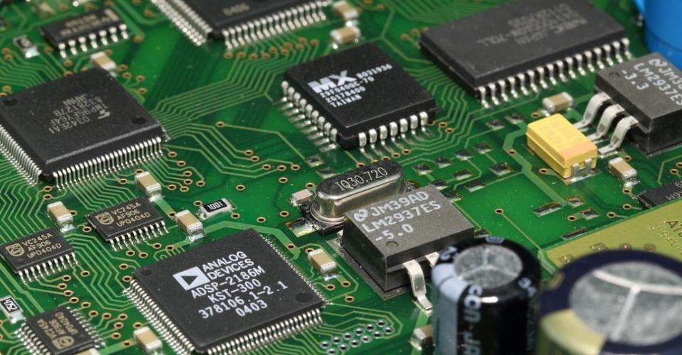
1.HDI
"The increase in the complexity of semiconductors and the total amount of logic gates has required integrated circuits to have more pins and finer pin pitches. В настоящее время на устройстве BGA спроектировано более 2000 зажимов (расстояние между выводами 1 мм), что является распространенным явлением, не говоря уже о размещении 296 штырей на устройстве с нулевым шагом.65mm. The need for faster and faster rise times and signal integrity (SI) requires a larger number of power and ground pins, so it needs to occupy more layers in the multi-layer board, Таким образом, приводя высокий уровень микропропускания. The need for density interconnection (HDI) technology.
HDI - технология взаимодействия, разработанная для удовлетворения этих потребностей. микропористый и сверхтонкий диэлектрик, finer traces and smaller line spacing are the main features of HDI technology.
2.RF design
For RF design, схема радиочастоты должна быть спроектирована непосредственно для схем системного принципа и планировки системной доски, and not used in a separate environment for subsequent conversion. Все симуляции, tuning and optimization capabilities of the RF simulation environment are still necessary, « исходные условия» более приемлемы для аналоговых данных, чем « реальная среда». Therefore, различия между моделями данных и возникающие в результате этого проблемы при их преобразовании исчезнут. First, конструктор может непосредственно взаимодействовать между проектированием системы и имитацией радиочастот; второй, if designers perform a large-scale or quite complex RF design, Они могут пожелать поручить моделирование схем нескольким вычислительным платформам, выполняющим параллельные работы, or They want to send each circuit in a design composed of multiple modules to their respective simulators, Таким образом уменьшать время моделирования.
3. Advanced packaging
The increasing functional complexity of modern products requires a corresponding increase in the number of passive components, which is mainly reflected in the increase in the number of decoupling capacitors and terminal matching resistors in low-power, высокочастотное применение. Although the packaging of passive surface mount devices has shrunk considerably after several years, при попытке достичь максимальной плотности результаты остаются одинаковыми. The technology of printed components makes the transition from multi-chip components (MCM) and hybrid components to SiP and PCBs that can be directly used as embedded passive components today. в процессе перехода, the latest assembly technology was adopted. например, the inclusion of a layer of impedance material in a layered structure and the use of series termination resistors directly under the uBGA package greatly improve the performance of the circuit. сейчас, embedded passive components can be designed with high precision, устранение дополнительных шагов обработки сварного шва лазерной чисткой. Wireless components are also moving in the direction of improving integration directly in the substrate.
4. Rigid flexible PCB
In order to design a жёсткий лист, необходимо учитывать все факторы, влияющие на процесс сборки. A designer cannot simply design a жёсткий лист Как твердый PCB, как жёсткий лист is just another rigid PCB. Они должны управлять сконструированной зоной изгиба, с тем чтобы проектная точка не вызывала разрыв и отслоение проводов из - за напряжения на поверхности изгиба. There are still many mechanical factors to consider, например, минимальный радиус изгиба, dielectric thickness and type, вес листового металла, copper plating, общая толщина цепи, number of layers, количество изогнутых листов.
Understand rigid flexible design and decide whether your product allows you to create a rigid flexible design.
5. Signal integrity planning
In recent years, непрерывно совершенствуются новые технологии, связанные с параллельными шинными структурами и дифференциальными структурами.
типы типичных проблем с проектированием параллельной шины и последовательного преобразования. The limitation of parallel bus design lies in system timing changes, например, смещение часов и задержка распространения. Due to the clock skew on the entire bus width, временные ограничения по - прежнему трудно проектировать. Increasing the clock rate will only make the problem worse.
С другой стороны, the differential pair structure uses an exchangeable point-to-point connection at the hardware level to realize serial communication. обычно, it transfers data through a one-way serial "channel", можно сложить, 2-, 4,0, 8-, 16,0, and 32-width configurations. каждый канал имеет один байт данных, so the bus can handle data widths from 8 bytes to 256 bytes, с помощью некоторых методов обнаружения ошибок можно сохранить целостность данных. However, из - за высокого уровня данных, возникли другие вопросы проектирования. Clock recovery at high frequencies becomes the burden of the system, Потому что часы требуют быстрой блокировки потока входных данных, для повышения устойчивости схемы к трясению, it is necessary to reduce the jitter from cycle to cycle. шум питания также создает дополнительные проблемы для конструктора. This type of noise increases the possibility of severe jitter, Это еще труднее открыть глаза. Another challenge is to reduce common mode noise and solve the problems caused by the loss effects of IC packages, панель PCB, cables and connectors.
6. The practicality of the design kit
USB, Разоружение, демобилизация и реинтеграция/DDR2, PCI - X, PCI-Express, RocketIO и другие средства проектирования, несомненно, помогут дизайнерам выйти в область новых технологий. The design kit gives an overview of the technology, описание, и трудности, с которыми столкнутся дизайнеры, далее смоделируется и как установить связь. Вместе с программой он предоставляет пояснительные документы, which provides designers with an opportunity to master advanced new technologies.