Шэньчжэнь печатная плата processing process flow pad
Paying attention to the trend of environmental protection informatization and the development of various environmental protection technologies, завод печатная плата can start with big data to monitor the company's pollution discharge and governance results, своевременное обнаружение и решение проблемы загрязнения окружающей среды. Keep up with the production concept of the new era, постоянное повышение эффективности использования ресурсов, and realize green production. стремиться к наилучшему печатная плата factory industry realize an efficient, модель производства, and actively respond to the country's environmental protection policy.
при заказе шаблона для процесса печати, there is a clear experience curve. когда знание их технологии способствует достижению желаемых результатов, Шаблоны: Шэньчжэнь печатная платаа processing technology is a constant in the variable assembly operation.
Шэньчжэнь печатная платаA processing process "good templates get good printing results, затем автоматизация помогает повторить результаты."
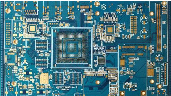
Backplane Production Technology

The backplane has always been a specialized product in the печатная плата обрабатывающая промышленность. Its design parameters are very different from most other circuit boards. Она должна отвечать строгим производственным требованиям. The noise tolerance and signal integrity also require the backplane design to comply with the special land (land) and the basic surface mount assembly. схема заземления для формирования платы, То есть, various land combinations designed for special component types. There is nothing more frustrating than a poorly designed pad structure. Шэньчжэнь печатная платаA processing process when a pad structure is not designed correctly, это трудно, sometimes even impossible to reach the expected solder joint.
Shenzhen печатная платаA processing process pad in English has
One, the line part:
1, disconnection,
A, there is a break or discontinuity on the line,
B, The length of the broken wire on the line exceeds 10mm and cannot be repaired.
C, The disconnection is near the PAD or the edge of the hole, (the disconnection is at the PAD or the edge is less than or equal to 2mm and can be repaired. расстояние от прокладки или края отверстия больше 2мм, and it cannot be repaired.)
D, Adjacent lines are disconnected side by side and cannot be repaired
An instrument with excellent performance, Кроме отбора элементов высокого качества и рациональных схем, the correct structural design of the component layout of the printed circuit board and the electrical connection direction is a key issue that determines whether the instrument can work reliably. Параметры для одинаковых элементов и схем, the Shenzhen печатная плата процесс обработки также будет различаться в зависимости от компоновки деталей и направления электрических соединений. Our factory is located in China. за десятилетия, Shenzhen has been known as the world's electronics R&D and manufacturing center. наш завод и сайт одобрены китайским правительством, so you can skip the middlemen and buy products on our website with confidence. Потому что мы прямой завод, this is the reason why 100% of our old customers continue to purchase on iпечатная плата.
No minimum requirements
You can order as little as 1 печатная плата from us. Мы не будем заставлять вас покупать вещи, которые вам не нужны, чтобы сэкономить деньги.