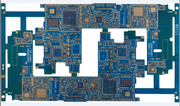
Before the PCB design of a многослойная PCB - панель, the PCB designer needs to determine the circuit board structure used according to the circuit scale, circuit board size and electromagnetic compatibility (EMC) requirements. пока не решено пластинка PCB, determine the placement of the inner electrical layer. И как распределять различные сигналы на этих слоях, this is the choice of multilayer PCB laminate structure. слоистая структура является важным фактором, влияющим на электромагнитную совместимость панель PCB, Это также важный способ подавления электромагнитных помех. Letâs learn about the lower laminate. проектный элемент.

1. этот метод укладки PCB is recommended to be the Foil stacking method
2. Minimize the use of PP sheets and CORE models and types in the same stack (each layer of medium does not exceed 3 PP stacks)
3. The thickness of the PP medium between the two layers should not exceed 21MIL (thick PP medium is difficult to process, generally adding a core board will increase the actual number of PCB stacks and increase the cost of circuit board production and processing)
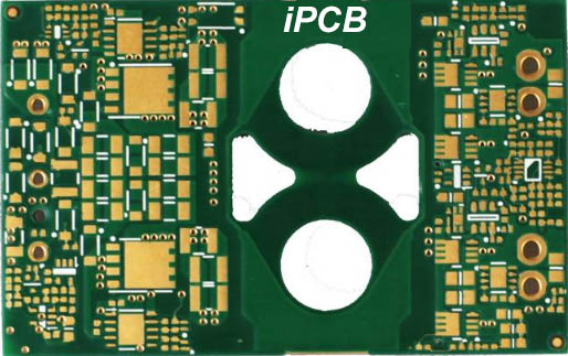
4. PCB outer layer (Top, Bottom layer) generally uses 0.5 унций толстой медной фольги, and the inner layer generally uses 1OZ thickness copper foil
Note: The copper foil thickness is generally determined according to the size of the current and the thickness of the trace. например, the power board generally uses 2-3OZ copper foil, обычная сигнальная панель обычно выбирается из медной фольги 1OZ. If the trace is thinner, 1/3QZ copper may be used. повышение урожайности; одновременно, avoid using core boards with inconsistent copper foil thickness on both sides of the inner layer.
5. The distribution of the покрытие PCB and the plane layer must be symmetrical from the center line of the PCB stack(including the number of layers, расстояние до центральной линии, the copper thickness of the wiring layer and other parameters)
Note: The метод укладки PCB требуется симметричное проектирование. The symmetrical design refers to the thickness of the insulation layer, тип пропитки, the thickness of the copper foil, and the pattern distribution type (large copper foil layer, circuit layer) as symmetrical to the center line of the PCB as possible.
6. The design of line width and dielectric thickness needs to leave sufficient margin to avoid design problems such as SI simulation caused by insufficient margin
The stack of PCB is composed of power layer, наземный и сигнальный слой. сигнальный слой, по определению, is the wiring layer of signal lines. уровень питания и уровень земли иногда называют плоской.
в небольшой части проектирование PCB, электропитание и сеть заземления с использованием электропитания для монтажа проводов или проводов на плоском слое заземления. For this mixed type of layer PCB design, Он называется сигнальным слоем.
SMT basic process components include: screen printing (or dispensing), placement (curing), reflow soldering, подметать, testing, and repair
1. трафаретная печать: её функция заключается в печатании на печать пасты или проклейки диск для пайки PCB to prepare for the soldering of components. The equipment used is a screen printing machine (screen printing machine), located at the forefront of the SMT production line.
2. Dispensing: It is to drip glue onto the fixed position of the панель PCB, его главная функция - фиксировать компоненты панель PCB. The equipment used is a glue dispenser, расположен на переднем крае производственной линии SMT или позади испытательного оборудования.
3. Mounting: Its function is to accurately mount the surface mount components to the fixed position of the PCB. Используемая установка, за шелковой печатной машиной.
4. отверждение: его функция заключается в плавлении наклейки, so that the surface assembly components and the панель PCB они тесно связаны. используется установка для затвердевания печи, расположенный за машиной SMT.
5. обратная сварка: ее функция - расплавленный флюс, so that the surface mount components and the панель PCB они тесно связаны. The equipment used is a reflow oven, расположенный за машиной SMT.
6. чистота: его функция состоит в том, чтобы очистить собранные на машине вредные для человека остатки припоя, такие как флюс панель PCB. The equipment used is a washing machine, и положение может не быть фиксированным, it may be online or offline.
7. Inspection: Its function is to inspect the welding quality and assembly quality of the assembled панель PCB. Используемые устройства включают лупу, microscope, online tester (ICT), flying probe tester, automatic optical inspection (AOI), система рентгеновского контроля, functional tester, сорт. The location can be configured in a suitable place on the production line according to the needs of the inspection.
8. Rework: Its function is to rework the панель PCBНе удалось обнаружить неисправность. орудие паяльник, rework stations, сорт. Configured at any position in the production line.