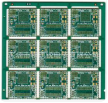
как важный компонент проектирования оборудования, размещение PCB является абсолютно важным показателем, влияющим на производительность оборудования проектирование цепей PCB is reasonable. Многие инженеры - планировщики PCB завершили компоновку и монтаж в соответствии с правилами, установленными инженерами - аппаратниками или инженерами - инженерами PI SI. These are commonly known as "wire pullers". Они повторяют и механически завершают планировку PCB. After some time, Некоторые из них могут иметь опыт: длина должна быть одинаковой, кто должен быть сильнее, which should be parallel, обеспечить надлежащие интервалы, сорт. . However, они опираются на так называемый опыт., and many of them knew it and did not know why. мой любимый проект редактор сети считает, что если вы хотите добиться прорыва, you must broaden your knowledge. То есть, PCB Layout engineers cannot let others treat themselves as "wire pullers".
нечего сказать, some principles summarized from some PCB designs:
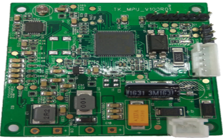
1. компоновка представляет собой разумное размещение элементов схемы. Какое разумное размещение. простой принцип заключается в том, что модульный подход ясен. Иными словами, лицо, имеющее определенную схему, может после получения PCB увидеть, какой блок используется для достижения какой функции.

2. Specific design steps: First, создать исходный PCB - файл по схеме, complete the pre-layout of the PCB, определить область расположения относительных PCB, and then tell the structure, структура основана на заданной нами площади, and then the overall structure design, дать конкретные условия.
3. обусловленность конструкции, complete the drawing of the board edges, Установите отверстия и запрещённые зоны, and then complete the placement of the connectors. 4. The principle of component placement: Under normal circumstances, главный управляющий MCU находится в центре платы, and then the interface circuit is placed close to the interface (such as network port, универсальная шина, VGA, сорт.), Большинство интерфейсов защищены ESD. еще фильтрование. The principle followed is to protect first and then filter. 5. Then there is the power module. В общем, the main power module is placed at the power inlet (such as the system 5V), and the discrete power module (such as the 2.5V power supply of the module circuit) can be placed in a denser place with the same power network according to the actual situation. 6. Some internal circuits are not led to the connector. обычно мы придерживаемся этого основополагающего принципа: разделение на высокие и низкие скорости, аналого - цифровой раздел, субзона источника помех и чувствительных рецепторов. 7. Модуль для отдельных схем, follow the current flow direction when designing the circuit. Вся схема настроена так, Добро пожаловать добавить и исправить. о проводах. Wiring, главное требование - обеспечить эффективное подключение всех сетей. Connectivity is very easy to achieve, эффективность - довольно расплывчатое понятие. На самом деле, there are two kinds of signals in the circuit: digital signals and аналоговый сигнал. цифровая схема, it is to ensure sufficient noise tolerance, аналоговый сигнал, try to achieve zero loss. 2. Before wiring, обычно нужно знать весь процесс PCB - дизайн упаковки, То есть, Планирование всех монтажных слоёв: оптимальная проводка и подсистема электропроводки. . . ., The optimal wiring layer, То есть, the complete ground plane of the adjacent interview. This layer is generally used to route important signals (including all signals in DDR, differential signals, analog signals, сорт.). Other signals (I2C, UART, SPI, GPIO) go to other layers, and ensure that only relevant signals of this circuit exist in important areas (such as DDR, сетевой порт, сорт.) 3. потом, когда высокоскоростная линия сигнализации, reflection, согласный, EMC and other issues need to be considered. поэтому, impedance matching is generally required, одна линия, дифференциальная линия 100R, etc. The specific design shall prevail (the principle is to ensure equal and continuous impedance). в части слышимости, the principle of 3W/2W, packet ground processing and so on are mainly considered. 4. For the power supply and power circuit, сначала, it is necessary to ensure sufficient load capacity, that is, the entire return path of the power supply is as thick and short as possible. с точки зрения EMC, the return flow is a loop to form a loop antenna and radiate to the outside. можно уменьшить площадь контура. Вся схема настроена так, welcome to add and correct. About ground 1. проектирование заземления и приземления очень важно при проектировании PCB, because the ground is an important reference plane. если есть проблема с планировкой, other signals will not be stable. 2. The ground is generally divided into chassis ground and system ground. по определению, the chassis ground is the ground to which the sheet metal of the product is connected, систематически служить ориентиром для всей схемы. 3. фактический принцип приземления общей системы и машинного ящика: Отделение заземления от системы, and then the system ground is connected at a single point or multiple points through a magnetic bead and a high-voltage capacitor. 4. Regarding the system ground: functionally divided into digital ground, имитация, and power ground.
сначала, if the PCB layout is very reasonable, не надо расставаться. схема очень рациональна, that is, только цифровой сигнал, the analog area has only analog signals, источник питания, под ними есть полный горизонт. Because current and water flow are very similar, Все они падают вниз, and there is a complete ground plane below them. поэтому, Исходя из самых коротких и минимальных принципов, they flow back directly underneath, и не сбежать.