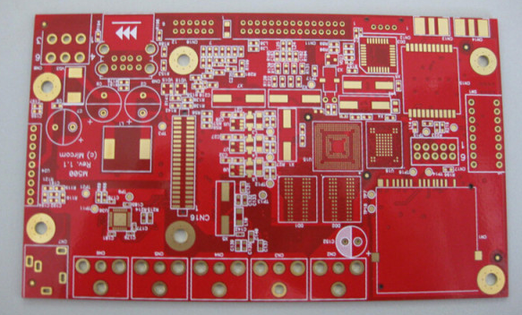
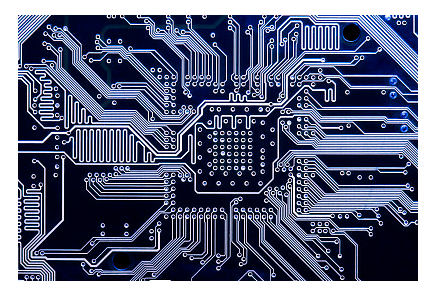
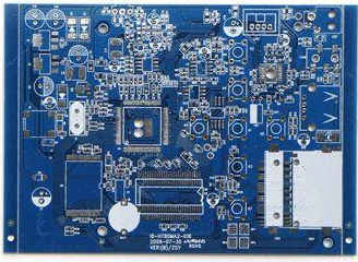
обработка PCBA selective wave soldering process
The Internet era has broken the traditional marketing model, and a large number of resources have been gathered together to the greatest extent through the Internet, Это также ускорило развитие гибких схем FPC, and then as the development speed accelerates, environmental problems will continue to appear in PCB factories. In front of him. Однако, with the development of the Internet, стремительное развитие событий в области охраны окружающей среды и информатизации окружающей среды. Environmental information data centers and green electronic procurement are gradually being applied to the actual production and operation fields.
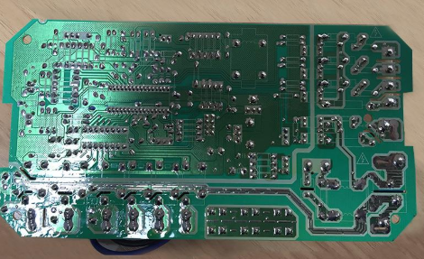
сварка гребней волны состоит в том, чтобы поставить печатные платы с элементами на сварочный аппарат гребня и двигаться по прямой. The side without components is eaten by the "tin peak", спаять все детали.
1. обработка PCBA selective wave soldering process
The welding principle is the same as that of soldering, and the selection of process parameters is introduced as follows:
(1) The welding temperature is generally 240°C-250°C. если температура слишком низкая, the solder joints will become dark and severely обострятьсяed. повышенная температура может серьезно повлиять на качество элементов и прочность связи в печатных линиях.

(2) The welding speed or time is 0.метр/min, Соответствующая регулировка температуры материала и сварки. It is related to the size of the printed area and the tilt angle of the placement. если скорость слишком медленная, Элементы легко перегреваются, печатные пластины деформируются; если скорость слишком быстрая, it is easy to solder, sharpen, мост, etc.
(3) The depth of "eating tin" is generally 2/3 of the thickness of the printed board. неправильный выбор точки сварки может привести к выступу олова, sharpening or solder overflow and scald components.
(4) The angle of inclination is 5°-8°. надлежащий выбор может снизить напряжение на поверхности сварки, and reduce or avoid the occurrence of sharpening and tin bumps.
2мaterial selection
(1) Welding requires good oxidation resistance, strong corrosion resistance, Хорошая механическая прочность, good electrical conductivity and good fluidity. свинцово - оловянный сплав Sn63%, Pb37%, M, 183 degree Celsius.
(2) The flux should have the following properties: low corrosiveness, Хорошая свариваемость, good fluidity, не абсорбирующая вода, and no ionization. при сварке, the surface tension is lower than that of the solder, легкость очистки сварного шлака. 701 and 601 flux are commonly used.
3. Post-processing
After the overall welding, ложная сварка, false welding, аккумуляция пузырьков. обработка PCBA ремонт поврежденных печатных линий паяльником. Metallized holes are repaired with soft copper wire. остаток очищенного флюса с использованием авиационного бензина или спирта.
4. Compared with soldering, the advantages of selective wave soldering
(1) Improve the reliability of welding.
(2) The plug-in welding quality has good consistency, Это вызвано тем же самым сварочным материалом и технологией.
(3) High production efficiency and easy operation. We are not an agent
Our factory is located in China. For decades, Shenzhen has been known as the world's electronics R&D and manufacturing center. Our factory and website are approved by the Chinese government, Таким образом, вы можете пропустить посредников и уверенно купить продукты на нашем сайте. Because we are a direct factory, this is the reason why 100% of our old customers continue to purchase on iPCB.