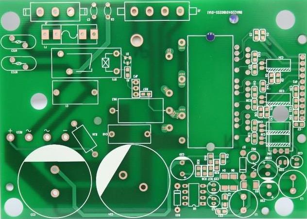
радиочастотная плата (RF)are called black art due to many uncertain factors. Однако, through practice and exploration, Мы найдём правила. The following will be based on our years of work practice and previous experience , Обсуждение плата цепиdesign of radio frequency circuits around these aspects: layout, импеданс, stacking, проектный соображение, edging, обработка питания, and surface treatment.
1 About layout
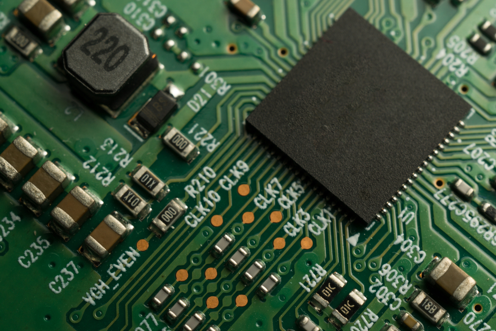
The principle of RF circuit layout is that the RF signal is as short as possible, и расстояние между входом и выходом далеко. The RF circuit is best arranged in a line, Следующий, it can be arranged in an L-shaped arrangement, or it can be arranged at an obtuse angle greater than 90 degrees (such as an angle of 135 degrees). There is also a U-shaped layout, это в основном зависит от потребностей в пространстве и проводке. The U-shaped layout is used when conditions are really limited, расстояние между двумя параллельными линиями как минимум 2 мм. устройство высокой чувствительности фильтра требует добавить металлический экран, and the place where the microstrip line enters and exits the shield must be slotted. RF area and other areas (such as voltage stabilizing block area, numerical control area) should be arranged separately; high-power amplifiers, low-noise amplifiers, частотный синтезатор, etc. нужно организовать отдельно, and they should be separated by barriers.
2 About impedance
Factors related to impedance are line width, thickness of dielectric plate, диэлектрическая постоянная диэлектрика, copper thickness and so on. на радиочастоте, 50 ohms is often used as the impedance matching standard. материал радиочастотной диэлектрической пластины обычно серии Роджерс, such as Rogers 4350 material. если мы выберем 0.254mm thickness, по аналогии, the line width is 0.55 мм, толщина меди 0.5OZ is selected, при этом можно управлять сопротивлением до 50 ом. For other models, Другие толщины листов могут имитироваться по их диэлектрической проницаемости и толщине. It is recommended that you use the Polar SI8000 impedance calculation tool for calculation, Просто и удобно.
3 About the stacked structure
The top layer of the RF board is generally placed with devices and microstrip lines. The second layer needs to be covered with a large area of network copper. дно должно быть полным горизонтом.. The copper layer should directly contact the cavity plane. требуется многослойный слой сигналов, поэтому между смежной линией сигнализации следует добавить пласт, двухслойная проводка должна быть вертикальной. Since the board cannot use non-ground network through holes, Другие сети, помимо заземленных отверстий, должны быть спроектированы с использованием слепых отверстий. If an eight-layer board, для эффективного использования стека, the seventh layer is preferably a signal line layer, Таким образом, будет много слепых отверстий от 1 до 7, in actual processing, эта конструкция слепой дыры вызовет серьезное коробление платы. Решение заключается в использовании противобурения, which is to make the blind hole according to the through hole, Удалить металл снизу вверх. Between the hole copper of the hole and the seventh and eighth layers, Не ходи на седьмой этаж. In order to make the performance more stable and eliminate the uncertainty, the hollow part can be filled with resin
4 Matters needing attention in плата цепиdesign
1) The duplexer, микшер и усилитель промежуточной частоты всегда имеют много радиопомех и сигналов промежуточной частоты, so the interference must be minimized. канал регистрации радиочастоты и промежуточной частоты должен быть как можно более пересекаться, и, насколько это возможно, положить между ними заземленную медь, and more grounding vias should be made.
2) Place as few non-ground vias as possible within 2 times the line width of the microstrip line of the RF board, and the size of the vias should be as small as possible, Это не только снижает индуктивность пути, so that the copper paving of the main ground plane will be as complete as possible and placed The RF signal energy is passed through the vias, causing leakage
3) The microstrip line of the radio frequency board should be windowed, that is, непроницаемая сварочная пленка без зеленого масла. The actual measurement shows that it has an improvement effect on the performance of the radio frequency circuit PCB.
4) A row of ground holes should be placed on the edge of the radio frequency signal at a distance of 1.в 5 раз параллельная ширина линии радиочастот. This distance should not be too close. Эмуляция показала, что если расстояние приземления слишком близко, частичная радиочастотная энергия будет связана. To the ground, Это может привести к определенным убыткам, the ground hole should be small and dense, диаметр обычно 0.2mm to 0.3 мм, and the distance is generally 0.6 мм - 1 мм. This ground hole can suppress the crosstalk between the microstrip lines. в реальной проводке, due to Some circuit boards have signal lines in the inner layer, и линия сложна, и часто бывает много мест, где невозможно установить раздельные отверстия. Then the solution is to change the ground hole that encounters the signal line to 1 to 2 blind holes. целостность геопористости получила большую защиту, and crosstalk is effectively suppressed

5 About hemming
The edging processing of the circuit board, обработка металлизации контуров радиочастот плата цепиcan reduce the loss of the radio frequency signal, потому плата цепиis made by jigsaw in the actual production process, Необходимо металлизировать край платы, вырезать края металлического покрытия перед потоком меди в отверстие. сейчас, the плата цепине завершено, Таким образом, плата должна быть соединена через некоторые связи, so it cannot be cut all. В общем, Мы считаем, что эти связки должны быть удалены от радиочастотной области и быть как можно короче. В общем, the board manufacturer will require two connecting straps on each side, и не менее 5 мм. Generally, микрополосная линия на входе и выходе радиочастоты должна быть сверху. при касании края доски, we will require the board factory to complete the edge at this position. Потому что края и земля в одной сети, it will be short-circuited with the microstrip line. Тогда нам нужно плата цепиto return to the process assembly department of our company. после, use a scalpel to gently scrape it away from the ground network. причина, по которой мы делаем это, заключается в том, чтобы держать края как можно более полными, and the connection belt is far away from the RF zone.
6 About the handling of radio frequency circuit board power
As we all know, питание цепи требует развязывающего конденсатора для фильтрации питания, чтобы устранить помехи. радиочастотный чип более чувствительный к питанию. Decoupling capacitors and isolation inductors are needed to filter the noise interference of the power supply. питание радиочастотной схемы должно быть введено сразу после платы. Perform filtering and distribute to various parts of the circuit by the voltage regulator block. чтобы уменьшить потери тока и вызвать падение давления, питание лучше передавать через слепую дыру внутреннего слоя на необходимое оборудование. питание радиочастотных схем обычно не делится на плоскость, and the whole block The power plane will interfere with the RF signal, Таким образом, ему просто необходимо выполнить текущие требования, чтобы он мог получить питание через внутренний слой. However, чтобы избежать падения напряжения, the power line should be as short as possible and not compatible with microstrip. перекрытие пути, but also to avoid loops. Кроме того, the decoupling power supply around the chip and the via holes on the grounding pad should be placed as close as possible to the capacitor pad, заземление конденсатора требует большой площади меди. Здесь следует отметить, что отверстие и количество отверстий должны выбираться в соответствии с текущим размером.
7 About surface treatment
RF boards often require gold wire bonding, обычная поверхностная обработка не может удовлетворить эти требования. Conventionally, гальваническое покрытия, and the gold thickness is controlled above 2um to achieve the adhesion requirements of gold wire bonding. многое зависит от чистоты. по технологическому требованию золочения, the pads must be physically connected, Так что все электроды можно гальванизировать. This appears between the two pads that should not be connected together in the плата PCBМы проектируем. есть очень тонкая технологическая линия, которую необходимо демонтировать вручную перед монтажом плата цепиis soldered. Это не только займет время, но и разрушит плавность и целостность линий. It is not realistic to leave the process line for complex multi-layer boards. на практике золочение, it is generally It is a method of pressing aluminum wire on the copper skin and then electroplating gold to remove the aluminum wire after gold plating. недостаток в этом заключается в том, что точки алюминиевого прессования не могут быть золочены. The electroless nickel-palladium-gold process has proven to achieve a perfect bonding effect and does not require a process line. Это может быть достигнуто путем регулирования толщины металла и никеля, palladium, золото. Nickel generally does not need special control according to the conventional thickness. толщина обычно контролируется на 3 микродюйма.