[IC Substrate manufacturer] этот whole process fromчип на интегральных схемахdesign, обрабатывающая промышленность упаковка
1 Complicatedчип на интегральных схемахdesign process
The process of chip обрабатывающая промышленность Да like building a house with LEGO. After the wafer is used as the foundation, and then the chip manufacturing process is stacked up layer by layer, the necessary чип на интегральных схемахs can be produced (these will be introduced later). Однако, without design drawings, it is useless to have strong manufacturing capacity. поэтому, the role of architects is very important. But who is the architect in IC design? Next, this paper will introduce the IC design.
в the IC production process, Большинство интегральных схем планируются и проектируются фирмой - специалистом по проектированию интегральных схем, such as MediaTek, Qualcomm, Интернет и другие известные производители, all design their own чип на интегральных схемахs and provide chips with different specifications and efficiency for downstream manufacturers to choose. Because IC is designed by each завод, IC design depends on the техника of engineers, качество инженера влияет на стоимость предприятия. Однако, when engineers design an чип на интегральных схемах, what are the steps? The design process can be simply divided into the following.

технология изготовления интегральных схем
Design the фёрст Step and Set Goals
In IC design, the most important step is specification. This step is like deciding how many rooms and bathrooms are required before designing the building, Какие строительные законы и правила, and designing after determining all functions, so as not to spend additional time on subsequent modifications. IC design also needs to go through similar steps to ensure that the designed chip will not have any errors.
The first step in specification formulation is to determine the purpose and efficiency of IC and set the general direction. The next step is to see which protocols to comply with. For example, the chip of the wireless network card needs to comply with IEEE 802.11 и другие характеристики. Otherwise, the chip will not be compatible with the products on the market, making it unable to connect with other devices. The last is to establish the implementation method of the IC, allocate different functions into different units, и установить связь между различными элементами, so as to complete the formulation of specifications.
After designing the specifications, the details of designing the chip are followed. This step is like writing down the architectural plan initially and drawing out the overall outline for the convenience of subsequent drawing. In чип на интегральных схемах, hardware description language (HDL) is used to describe the circuit. обычный HDL включает Verilog, VHDL, etc. the function of an IC can be easily expressed by code. затем Проверьте правильность функций программы и продолжайте изменять их до тех пор, пока не будет выполнено необходимое.

Пример 32 - разрядного сумматора
пользоваться компьютером, everything becomes Easy
With a complete plan, the next step is to draw a board design blueprint. In IC design, the step of logic synthesis is to put the determined HDL code into the electronic design automation tool (EDA tool), and let the computer convert the HDL code into logic circuit to produce the following circuit diagram. потом, repeatedly determine whether the logic gate design drawing meets the specifications and modify it until the function is correct.

Results of control unit synthesis
наконец, Включить код синтеза в другой набор инструментов EDA, используемых для компоновки, размещения и монтажа схем. After continuous detection, формирование следующей схемы. на фото, you can see different colors such as blue, red, green and yellow. Each different color represents a light mask. As for how to use the mask?

layout and winding
Layers of masks, stacked a chip
сначала, it is known that an IC will produce multiple masks. These masks have upper and lower layers, каждый этаж имеет свою задачу. The following figure is a simple mask example. Taking CMOS, the most basic element in integrated circuits, as an example, the full name of CMOS is complementary metal oxide semiconductor, То есть, combining NMOS and PMOS to form CMOS. As for what is metal oxide semiconductor (MOS)? This kind of component widely used in the chip is difficult to explain, простому читателю трудно понять. I won't study it more here.
Как показано на диаграмме ниже, the left side is the circuit diagram formed after circuit layout and winding. It has been known that each color represents a mask. правая сторона разворота каждого капота. обрабатывающая промышленность должна начинаться с нижнего слоя, follow the method proposed in the previous article on the manufacturing of чип на интегральных схемахs, делать этажом, and finally produce the desired chip.

до сих пор, we should have a preliminary understanding of IC design. On the whole, it is clear that IC design is a very complex specialty. Thanks to the maturity of computer-aided software, IC design can be accelerated. The IC design factory relies heavily on the wisdom of engineers. Each step described here has its own expertise and can be independently divided into multiple professional courses. For example, writing hardware description language is not simple. It only needs to be familiar with the programming language, но также нужно понять, как работает логическая схема и как преобразовать необходимые алгоритмы в программу, как синтезированное программное обеспечение преобразует программу в логическую.
Что такое вафли?
In the news of semiconductors, Мы всегда говорили о « вафельных» установках с масштабом, such as 8-inch or 12-inch wafer factories. Однако, what is the so-called wafer? какая часть 8 дюймов? How difficult is it to produce large-size wafers? The following is a step-by-step introduction to the most important foundation of Semiconductors - what is "wafer".
Wafers are the basis for manufacturing all kinds of computer chips. Мы можем построить дом из чипсов, and complete our desired shape (that is, all kinds of chips) by stacking layer after layer. However, if there is no good foundation, the built house will be crooked, Это не то, чего ты хочешь. In order to make a perfect house, Тебе нужна стабильная основа. For chip manufacturing, this substrate is the wafer to be described next.

First of all, let's recall that when we played with high-rise blocks as children, поверхность массива будет иметь небольшую круговую проекцию. With this structure, Мы можем складывать два кирпича без клея.. Chip manufacturing also fixes the subsequently added atoms and the substrate together in a similar way. поэтому, we need to find a substrate with neat surface to meet the conditions required for subsequent manufacturing.
In solid materials, there is a special crystal structure - single crystal. It has the characteristic that atoms are closely arranged one by one, and can form a flat atomic surface. поэтому, the above requirements can be met by using single crystal to make wafers. However, how to produce such a material? Основные два шага: очистка и рисование кристаллов, and then such a material can be completed.
How to make a single crystal wafer
The purification is divided into two stages. The first step is metallurgical purification. процесс заключается в основном в поглощении углерода, конверсии окиси кремния в кремний с чистотой более 98% на основе окислительного восстановления. Most metal refining, железо или медь, uses this method to obtain metal of sufficient purity. However, 98% по - прежнему недостаточно для изготовления чипов, и необходимы дальнейшие улучшения. поэтому, Siemens process will be further used for purification. такой, high-purity polysilicon required by semiconductor process will be obtained.

технология изготовления кремниевых колонн
The next step is crystal drawing. First, the high-purity polysilicon obtained above is melted to form liquid silicon. Then, contact the liquid surface with a single crystal seed and slowly pull it up while rotating. зачем нужен монокристаллический кремний, it is because the arrangement of silicon atoms is the same as that of people in line. It will need a leader to let later people know how to arrange correctly. Silicon seeds are an important leader to let later atoms know how to queue. Finally, after the silicon atoms leaving the liquid surface solidify, the neatly arranged monocrystalline silicon columns are completed

Monocrystalline silicon column
However, what do 8 inches and 12 inches represent? Он имел в виду диаметр кристаллической колонны, которую мы производим, which looks like the part of the pencil holder. обработанные поверхности и разрезанные на тонкие пластины. What is the difficulty of making large-size wafers?
As mentioned above, the manufacturing process of crystal column is like making cotton candy, одновременное вращение и формование. If you have ever made marshmallows, you should know that it is very difficult to make large and solid marshmallows, and the process of crystal drawing is the same. The speed of rotation and temperature control will affect the quality of crystal column. поэтому, the larger the size, the higher the requirements for speed and temperature. Therefore, it is more difficult to make high-quality 12 inch wafers than 8-inch wafers.
However, a whole silicon column can not be made into a substrate for chip manufacturing. In order to produce silicon wafers one by one, it is necessary to cut the silicon column horizontally into wafers with a diamond knife, затем полировка кремниевых пластин, формирование кристаллов для изготовления необходимых кремниевых пластин. After so many steps, the manufacturing of chip substrate выполнить. The next step is to stack houses, that is, chip manufacturing. As for how to make chips?
Layers of stacked chips
After introducing what silicon wafers are, I also know that manufacturing чип на интегральных схемахs is like building a house with Lego blocks, creating the desired shape by stacking layer after layer. However, there are quite a few steps to build a house, and so are IC manufacturing. What are the steps to manufacture IC? This paper will introduce the process ofчип на интегральных схемахmanufacturing.
Before we begin, we should first understand whatчип на интегральных схемахis. IC, the full name of integrated circuit, can be seen from its name that it combines the designed circuits in a stacked manner. Таким образом, we can reduce the area required to connect the circuit. схема ис 3D. видно, что его конструкция похожа на балки и столбы дома., stacked layer by layer, which is why IC manufacturing is compared to building a house.

3D profile of чип на интегральных схемах
From the 3D profile ofчип на интегральных схемахin the figure above, the dark blue part at the bottom is the wafer introduced in the previous article. из этого числа, we can know more clearly how important the wafer substrate plays in the chip. Что касается красных и хакерских частей, they are to be completed during IC production.
First of all, the red part can be compared to the hall on the first floor of a high-rise building. The hall on the first floor is the gateway of a house. It is where people go in and out. It usually has more functionality under the control of traffic. Therefore, compared with other floors, the construction will be more complex and require more steps. In the IC circuit, this hall is the logic gate layer, which is the most important part of the whole IC. комбинация комбинирование нескольких логических элементовчип на интегральных схемахwith complete functions.
The yellow part is like a general floor. Compared with the first floor, it will not have too complex structure, во время строительства каждый этаж не будет сильно меняться. этот слой предназначен для соединения логических дверей в красной части. The reason why so many layers are needed is that there are too many lines to be connected together. When a single layer cannot accommodate all lines, it is necessary to stack several layers to achieve this goal. In this process, the lines of different layers will be connected up and down to meet the wiring requirements.
Layered construction and layer by layer structure
After knowing the structure of IC, we will introduce how to make it. Imagine that if we want to make a fine drawing with a paint spray can, Нам нужно вырезать графическую крышку и накрыть её на бумагу.. Then spray the paint evenly on the paper. After the paint is dry, remove the shutter. After repeating this step, neat and complex graphics can be completed. Manufacturing IC is to stack layer by layer by covering in a similar way.
When making IC, it can be simply divided into the above four steps. Although the manufacturing steps and materials used are different in actual manufacturing, similar principles are generally adopted. This process is a little different from paint painting. IC manufacturing is first coated and then covered, while paint painting is first covered and then painted. Each process is described below.
-Metal splashing: evenly sprinkle the metal material to be used on the wafer to form a thin film.
-Coating photoresist: first place the photoresist material on the wafer, pass through the mask (the principle of the mask will be explained next time), hit the beam on the unwanted part, and destroy the structure of the photoresist material. Then, the damaged materials are washed away with chemicals.
-Etching technology: the silicon wafer without photoresist protection is etched by ion beam.
-Photoresist removal: dissolve the remaining photoresist using the photoresist removal solution, so as to complete a process.
Finally, many чип на интегральных схемахs will be completed on a whole wafer. Next, as long as the completed square чип на интегральных схемахs are cut off, they can be sent to the упаковка завод упаковка. What is the упаковка factory? I'll explain later.

Comparison of wafers of various sizes
3 What is the nanofabrication process?
Samsung and TSMC are very hot in the advanced semiconductor manufacturing process. They both want to take the lead in wafer foundry to win orders. это почти стало полемикой между 14nm и 16nm. However, what is the meaning of the two numbers of 14nm and 16nm, and which part does it refer to? What benefits and problems will it bring in the future after reducing the process? We will briefly explain the nano process below.
How subtle isнанотехнология?
Before we start, we should first understand what nano means. Mathematically, the nanometer is 0.000000001 meters, Но это очень плохой пример.. After all, we can only see many zeros after the decimal point, but we don't have a practical feeling. если сравнить толщину ногтей, it may be more obvious.
если вы действительно измеряете линейкой и калибром, Вы можете знать толщину ногтей около 0.0001 meter (0.1 mm), that is, Попробуйте разрезать ребро гвоздя на 100 000 линий, каждая линия соответствует примерно 1 нанометр. Therefore, you can imagine how small нанометр is.
после того, как стало известно, насколько маленькими были нано, we should also understand the intention of reducing the process. сокращение транзисторов в основном направлено на то, чтобы увеличить число транзисторов, вставляемых в более мелкие чипы, Таким образом, Чип не будет расти из - за технического прогресса; Следующий, it can increase the operation efficiency of the processor; Moreover, reducing the volume can also reduce the power consumption; Finally, после уменьшения кристалла, it is easier to plug it into the mobile device to meet the needs of lightweight in the future.
Then come back to explore what the nano process is. Take 14 nm as an example. процесс означает, что минимальный провод в кристалле может достигать 14 нанометров. The following figure shows the appearance of traditional transistors as an example. главная цель сокращения транзистора заключается в снижении энергозатрат, but which part should be reduced to achieve this purpose?
The L in the lower left figure is the part we expect to shrink. By reducing the gate length, the current can use a shorter path from the drain end to the source end (если вас интересует, you can use Google to search for MOSFET, which will be explained in more detail).

Кроме того, компьютер работает на 0 и 1. How can transistors meet this purpose? метод определения тока на транзисторах. When voltage is supplied at the gate terminal (Green Square), ток от зажима стока к зажиму истока. If no voltage is supplied, the current will not flow, so it can represent 1 and 0ï¼ As for why we use 0 and 1 for judgment, if you are interested, you can check brin algebra. Мы этим способом делаем компьютеры..)
Size reduction has its physical limitations
However, the manufacturing process cannot be reduced indefinitely. When we reduce the transistor to about 20 nm, мы столкнемся с проблемами в квантовой физике, so that the transistor has leakage, offsetting the benefits obtained when l is reduced. As an improvement method, the concept of FinFET (tri gate) is introduced, as shown in the upper right figure. In the previous explanation made by Intel, it can be known that the introduction of this technology can reduce the leakage caused by physical phenomena.

More importantly, this method can increase the contact area between the gate end and the lower layer. In the traditional practice (above left), the contact surface has only one plane, but after using FinFET (tri gate) technology, поверхность контакта станет трехмерной, which can easily increase the contact area. такой, the source drain end can be made smaller while maintaining the same contact area, Это очень помогло уменьшить размер.
Finally, Вот почему некоторые говорят, что крупные заводы столкнутся с серьезными проблемами при переходе на 10 нанотехнологий.. The main reason is that the size of an atom is about 0.1 nm. In the case of 10 nm, на одной прямой меньше 100 атомов, which is quite difficult to manufacture, and as long as there is a defect of one atom, such as atoms falling out or impurities in the manufacturing process, There will be an unknown phenomenon, which will affect the yield of the product.
If you can't imagine the difficulty, you can do a small experiment. Поставьте десятичную и сто перьев на стол. десять квадратов, and cut a piece of paper to cover the beads, then brush off the next beads with a small brush, and finally make him form a 10 Ã A rectangle of 5. In this way, we can know the difficulties faced by major factories and how difficult it is to achieve this goal.
As Samsung and TSMC will complete the mass production of 14 nm and 16 nm FinFET in the near future, they both want to compete for the OEM of Apple's next-generation iPhone chip. We will see quite wonderful commercial competition and obtain more power-saving and lightweight mobile phones. Благодаря Закону моля.
4 Tell you what encapsulation is
Packaging, final protection and integration of чип на интегральных схемах
After a long process, от проектирования до изготовления, we finally got an чип на интегральных схемах. However, a chip is quite small and thin. If it is not protected outside, it will be easily scratched and damaged. In addition, because the size of the chip is small, если не большая оболочка, поместить её вручную на платы не так легко. Therefore, Эта статья описывает и описывает упаковка next.
сейчас, there are two common packages, one is the dip package common in electric toys, which looks like a centipede in black, and the other is the BGA package common when buying boxed CPU. Что касается других упаковка methods, PGA (pin grid array) used by early CPUs; Pin grid array) or improved QFP (plastic square flatpack) of dip. Потому что так много упаковка methods, dip and BGA упаковка will be introduced below.
Traditional упаковка, lasting
The first thing to introduce is the dual inline package; Dip), Как показано на диаграмме ниже, the чип на интегральных схемах Эта посылка будет выглядеть как черная сколопендра, соединённая в две шеренги под ногами, Впечатляет. This упаковка method is the earliest IC упаковка technology, which has the advantage of low cost and is suitable for small chips without too many wires. However, Потому что большинство из них пластмассы, the heat dissipation effect is poor, which can not meet the requirements of current high-speed chips. Therefore, most of the chips using this package are enduring chips, such as op741 in the figure below, or чип на интегральных схемахнизкий спрос на скорость эксплуатации, smaller chips and fewer connection holes.

Amplifier cross-sectional view
As for ball grid array (BGA) упаковка, compared with dip, the упаковка volume is smaller and can be easily put into smaller devices. In addition, because the pin is located below the chip, it can accommodate more metal pins than dip, which is quite suitable for chips requiring more contacts. However, this упаковка method has high cost and complex connection method, so it is mostly used in products with high unit price.

The schematic diagram of BGA using flip chip упаковка
With the rise of mobile devices, new technologies have leapt onto the stage
However, using these упаковка methods will consume a considerable volume. For example, mobile devices and wearable devices now require quite a variety of components. если каждый компонент является самостоятельным, it will consume a lot of space to combine. Therefore, there are two methods to meet the requirements of reducing volume, namely SOC (system on chip) and SIP (system in packet).
At the beginning of the rise of smart phones, слово SOC можно найти в главном финансово - экономическом журнале. However, what is SOC? In short, Это преобразование IC с различными функциями в один чип. This method can not only reduce the volume, but also reduce the distance between different ICs and improve the computing speed of the chip. Что касается способа изготовления, it is to put different ICs together in the IC design stage, and then make a mask through the design process described earlier.
However, SOC does not have only advantages. разработка SOC требует значительного технического сотрудничества. When чип на интегральных схемах are packaged, they are protected by external упаковка, and the distance between IC and IC is far, so there is no mutual interference. However, when all ICs are packaged together, it is the beginning of the nightmare. The IC design factory should change from the original simple design IC to an IC that understands and integrates various functions, увеличить рабочую нагрузку инженера. In addition, there will be many situations, such as the high-frequency signal of the communication chip may affect the IC of other functions.
In addition, SOC also needs to obtain IP (intellectual property) authorization from other manufacturers to put components designed by others into SOC. Because the fabrication of SOC requires the design details of the whole IC to make a complete mask, which also increases the design cost of SOC. Some people may question why not design one yourself? Because designing various ICs requires a lot of knowledge related to the IC, only companies with a lot of money like apple can have a budget to recruit top engineers from well-known enterprises to design a brand-new IC. Сотрудничество и делегирование полномочий эффективнее с точки зрения затрат, чем разработка собственных IC.
Compromise, SIP appears
As an alternative, SIP прыгнула на сцену со встроенным чипом. Different from SOC, it purchases various IC's and encapsulates them for the last time, Таким образом, устранены этапы IP - авторизации, что значительно снижает затраты на проектирование. In addition, because they are independent ICs, the degree of interference with each other is greatly reduced.

Apple watch использует SIP
The most famous products using SIP technology are apple watch. Because the internal space of the watch is too small, it cannot adopt traditional technology, and the design cost of SOC is too high, SIP has become the first choice. использовать технологию SIP, it can not only reduce the volume, but also shorten the distance between each IC, which has become a feasible compromise. The following figure is the structure diagram of Apple watch chip. You can see that a considerable number of ICs are included in it.

Internal configuration diagram of S1 chip
After the упаковка is completed, it is necessary to enter the testing stage. На данном этапе, it is necessary to confirm whether the packaged IC operates normally. После правильного, it can be shipped to the assembly plant to make the electronic products we see. So far, the semiconductor industry has completed the whole production task.
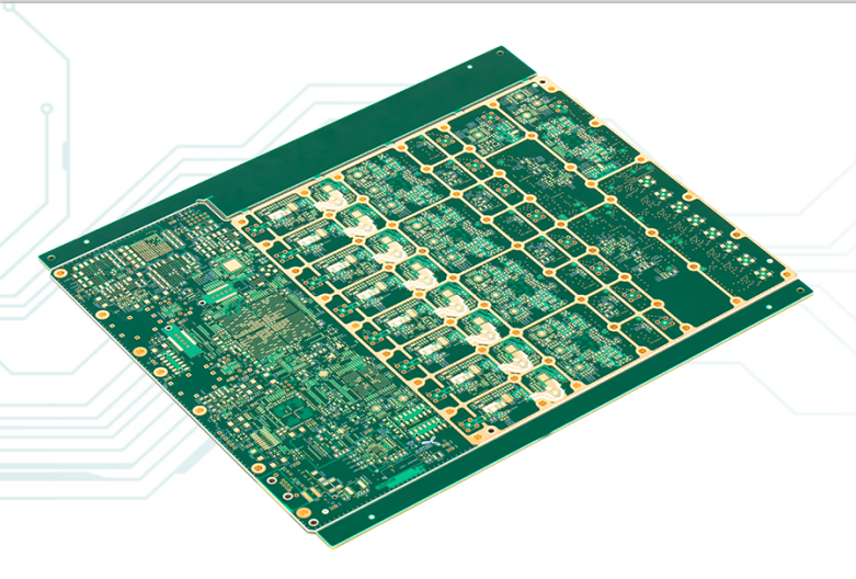
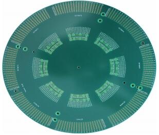
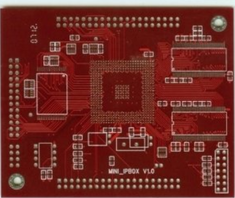
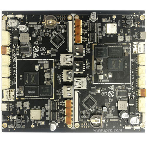
It is a professional R & D and manufacturer of high-precision PCB плата цепи. It can mass produce 4-46 layers of PCB boards, circuit boards, circuit boards, high-frequency boards, быстродействующая плата, HDI boards, PCB circuit boards, high-frequency high-speed boards, IC упаковка несущая плита, semiconductor test boards, multilayer circuit boards, HDI circuit boards, плата смешанного напряжения, high-frequency circuit boards, soft and hard combination boards, etc