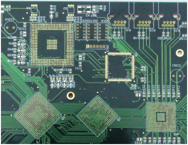
высокоточная печатная схема означает использование тонкой ширины линии/spacing, микропористость, narrow ring width (or no ring width), а также погребенные и слепые отверстия для достижения высокой плотности. And high precision means that the result of "fine, маленький, narrow, "тонкий" неизбежно приведет к высоким требованиям точности. Take the line width as an example: O.ширина линии 20 мм, O.D. is produced according to regulations. 15815½ * 0.24mm is qualified, and its error is (O. 20 ± 0.04) mm; and O. For a line width of 10mm, the error is (0."10 ± 0".02)mm. очевидно, the accuracy of the latter is increased by a factor of 1, не трудно понять, so the high-precision requirements will not be discussed separately. Но это одна из наиболее важных проблем в производственной технологии..

(1) Fine wire техника будущее, ширина тонкой проволоки/расстояние увеличится с 0.20mm-O. только 13 мм - 0.08mm-0.005mm can meet the requirements of SMT and Multichip Package (MCP). поэтому, the following technology is required.
использование тонкой или тонкой медной фольги (< 18Угу.) и тонкой поверхностной обработки.
использование более тонких сухих и влажных пленок, тонких и высококачественных сухих мембран может уменьшить искажения и дефекты ширины линий. влажная мембрана может заполнять небольшие газовые зазоры, увеличивая межфазную адгезию, увеличивая целостность и точность проводов.
3. Using parallel light exposure technology. Потому что параллельная фотоэкспозиция может преодолеть влияние изменения ширины линии, вызванного наклонным лучом точечного источника света, it is possible to obtain fine wires with precise line width dimensions and smooth edges. Однако, the parallel exposure equipment is expensive, высокая инвестиция, and it is required to work in a high cleanliness environment.
4. Electrodeposited Photoresist (Electro-deposited Photoresist, ED) is used. Its thickness can be controlled in the range of 5-30/um, which can produce more perfect fine wires. Он особенно применим к более узкому кольцу, no ring width and full plate electroplating. В настоящее время в мире насчитывается около дюжины производственных линий ED.
5. Using automatic optical inspection technology (Automatic Optic Inspection, AOI). Эта техника стала незаменимым средством контроля в производстве тонкой линии., and is rapidly being promoted, применение и разработка.
(2) Microporous technology The functional holes of the printed circuit board used for surface mounting are mainly used for electrical interconnection, Это делает применение микропористости более важным. The use of conventional drill materials and CNC drilling machines to produce tiny holes has many failures and high costs. поэтому, the high-density of printed boards is mostly focused on the refinement of wires and pads. Несмотря на огромные успехи, его потенциал ограничен. To further improve the densification (such as wires less than 0.08mm), the cost is urgent. поэтому, it turns to use micropores to improve the densification.
В последние годы, numerical control drilling machines and micro-drill technology have made breakthrough progress, Поэтому техника микропористости развивается быстро. This is the main outstanding characteristic in the current printed board production. In the future, the micro-hole forming technology will mainly rely on advanced CNC drilling machines and excellent micro-heads, с точки зрения себестоимости и качества отверстий, лазерная техника по - прежнему образует меньше дырок, чем цифровые управляемые сверлильные станки..
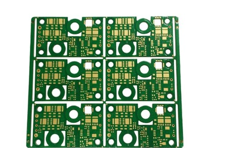
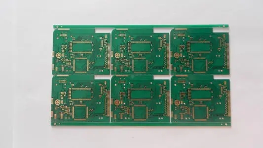
1. Buried, слепой, and through-hole technology The combination of buried, слепой, and through-hole technology is also an important way to increase the density of printed circuits. В общем, the buried and слепой holes are all tiny holes. Помимо увеличения количества соединений на платы, the buried and blind holes are interconnected by the "nearest" inner layer, это значительно снижает количество образующихся отверстий, and the setting of the isolation disk will also be greatly reduced. уменьшение, thereby increasing the number of effective wiring and inter-layer interconnection in the board, и повышенная плотность межсоединений. поэтому, сочетание многослойных пластин с погруженными трубами, blind, плотность межсоединений через отверстие при одинаковых размерах и слоях не менее чем в три раза превышает традиционную структуру целых отверстий.. If the buried, blind, and The size of the printed board combined with through holes will be greatly reduced or the number of layers will be significantly reduced. поэтому, in high-density surface-mounted printed boards, все шире применяются технологии погружения и слепого отверстия, монтаж печатных плат не только на поверхности большого компьютера, communication equipment, сорт., but also in civil and industrial applications. Она также широко используется в этой области, even in some thin boards, как тонкие шестислойные панели, такие как PCMCIA, Smard, ICCA.
печатные платы с утопленными и слепыми отверстиями, как правило, изготавливаются методом "поддона", Это означает, что они должны быть выполнены многократно нажимая вниз, drilling, покрытие отверстием, so precise positioning is very important .
2. Numerical control drilling machine At present, технологии цифрового сверлильного станка получили новый прорыв и прогресс. And formed a new generation of CNC drilling machine characterized by drilling tiny holes. The efficiency of drilling small holes (less than 0.50mm) of the micro-hole drilling machine is 1 times higher than that of the conventional CNC drilling machine, меньше неудач, and the rotation speed is 11-15r/беспокоить Может быть в 0. 1ï½0.2 мм, using high-quality small drills with high cobalt content, three plates (1.6 мм/block) can be stacked for drilling. когда сверло сломано, it can automatically stop and report the position, automatically replace the drill bit and check the diameter (the tool library can hold hundreds of pieces), and can automatically control the constant distance between the drill tip and the cover and the drilling depth, чтобы можно бурить слепое отверстие, It will not damage the countertop. магнитная суспензия на воздушной подушке, which can move faster, зажигалка, and more accurately without scratching the surface. Эта буровая установка в настоящее время пользуется большим спросом, such as the Mega 4600 from Prurite in Italy, Excelion 2000, and new generation products from Switzerland and Germany.
3. There are indeed many problems with laser drilling conventional CNC drilling machines and drill bits to drill tiny holes. Он препятствует развитию технологии микропористости, so laser ablation has received attention, Исследования и применение. But there is a fatal shortcoming, То есть, the formation of a horn hole, с увеличением толщины плит ситуация становится еще более серьезной. Coupled with high-temperature ablation pollution (especially multi-layer boards), the life and maintenance of the light source, повторяемость коррозионных отверстий, and the cost, сорт., распространение и применение микроотверстий в производстве печатных плат ограничено. Однако, лазерная абляция все еще используется для тонкой и плотной микропористой пластины, especially in MCM-L's high-density interconnect (HDI) technology, например, M ïcq. The polyester film etching hole in Ms and the metal deposition (sputtering technology) are combined in high-density interconnection. The formation of buried vias in high-density interconnection multilayer boards with buried and blind via structures can also be applied. However, due to the development and technological breakthroughs of CNC drilling machines and micro-drills, Они быстро получили распространение и применение. Therefore, the application of laser drilling in surface mount printed boards cannot form a dominant position. Но она все еще имеет место в одной области.
The above is the introduction of high-density производство PCB technology. Ipcb also provides PCB manufacturers and PCB manufacturing technology.