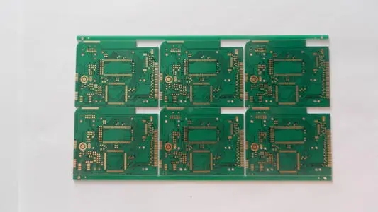
плата PCB production process and PCB manufacturing process
The inventor of the printed circuit board was Paul Eisler, австриец, who used the printed circuit board in a radio device in 1936. 1943 год, the Americans used this technology extensively in military radios. 1948 год, the United States officially recognized this invention for commercial use. с середины 50 - х годов хх века, printed circuit board technology has only begun to be widely adopted.

Перед появлением печатной платы, the interconnection between electronic components was achieved by direct connections. Но сейчас, the circuit panel only exists as an effective experimental tool; the printed circuit board has occupied an absolute dominant position in the electronics industry.
1. Detailed explanation of relevant design parameters:
one. line
1. Minimum line width: 6mil (0.153mm). That is to say, Если ширина линии меньше 6 мил, Она не сможет. If the design conditions permit, Чем больше проект, the better, Чем больше ширина линии, лучше завод, the higher the yield, а генерал проектирование PCB около 10 миль в день. This is very important, and the design must be consider
2. Minimum line spacing: 6mil (0.153mm). The minimum line distance is line-to-line, расстояние линии до паяльного диска не менее 6 мил. From the production point of view, Чем больше, the general rule is 10mil. Конечно, if the design is conditional, Чем больше. This is very important. Design Must consider
3. The distance between the line and the outline line is 0.508mm (20mil)
two. via via (commonly known as conductive hole)
1. минимальный диаметр отверстия: 0.3mm (12mil)
2. The minimum via hole (VIA) aperture is not less than 0.3mm (12mil), and the single side of the pad cannot be less than 6mil (0.153mm), preferably greater than 8mil (0.2mm), but not limited (see Figure 3) Это очень важно, The design must be considered
3. The via hole (VIA) hole-to-hole spacing (hole side to hole side) cannot be less than: 6mil, preferably greater than 8mil. This point is very important, and the design must be considered
4. расстояние между паяльной плиткой и профильной линией составляет 0.508mm (20mil
Third, the production process
Double-sided tin plate/immersion gold plate production process: cutting-drilling--sinking copper-circuit-drawing electricity-etching-solder mask ---Character----Spray tin (or heavy gold)-Gong edge-V cut (some boards donât need)-----Fly test----Vacuum packaging
Multi-layer tin board/immersion gold board production process: cutting-inner layer--lamination-drilling--sinking copper-circuit--map electricity- ---Etching-----Solder Mask---Character----Spray Tin (or Immersion Gold)-Gong Edge-V Cut (Some Boards Not Needed)-----Fly Test---- Vacuum packaging