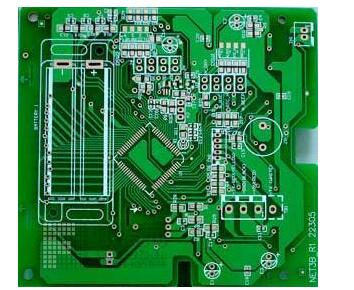
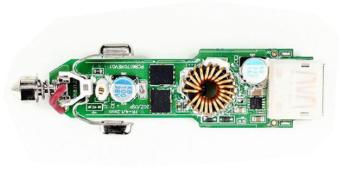
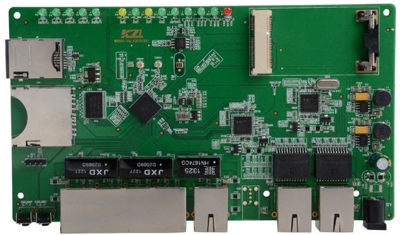
сварка PCBA процессing requirements for панель PCB
Когда? сварка PCBA is processed, обычно есть много требованийпанель PCBA, and the board must meet the requirements to accept welding processing. Так зачем же технология сварки требует так много требований к платы? It turns out that in the process of PCBA processing, будет много особых процессов, and the application of special processes immediately brings requirements for the PCB board. если у PCB - панелей проблемы, it will increase the difficulty of the PCBA soldering process, Окончательный дефект сварки, unqualified boards, сорт. Therefore, для обеспечения успешного завершения специальной технологии, удобная технология сварки PCBA, the PCB board must meet the manufacturability requirements in terms of size and pad distance. а сегодня покажу вам, как правильно работает технология пайки PCBA. The requirements of the PCB board.

1. PCB size
The width of the PCB (including the edge of the board) should be greater than 50mm and less than 460mm, and the length of the PCB (including the edge of the board) should be greater than 50mm. If the size is too small, нужно сделать мозаику.
2. PCB board edge width
Board edge width: >5 мм, panel spacing: <8mm, distance between pad and board edge: >5mm
3. PCB bending
Upward bending degree: <1.2 мм, downward bending degree: <0.5mm, PCB distortion: maximum deformation height ÷ diagonal length <0.25
4.PCB метка панели
Mark shape: standard circle, площадь, triangle;
Mark size: 0.8 ~ 1.5mm;
Mark material: gold-plated, лужение, copper and platinum;
Mark's surface requirements: the surface is flat, гладкий, non-oxidized, and free of dirt;
Mark's surrounding requirements: there should be no green oil or other obstacles within 1mm, which is obviously different from the Mark's color;
Mark position: 3mm above the edge of the board, не должно быть такой отметки, test points, сорт. within 5mm around the board.
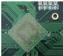
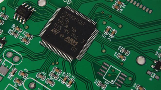
5. PCB pads
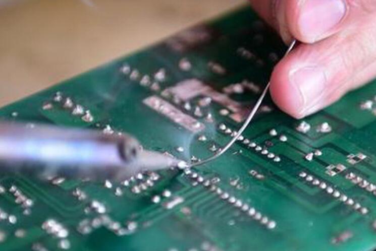
There are no through holes on the pads of SMD components. если есть сквозное отверстие, the solder paste will flow into the hole, привести к меньшему количеству олова в оборудовании, or the tin flowing to the other side, вызывает неровность поверхности платы, не может быть напечатана паста.
When conducting PCB design and production, it is necessary to understand some knowledge of сварка PCBA process, so as to make the product suitable for production. Во - первых, понимание требований перерабатывающих заводов может сделать последующий производственный процесс более плавным и избежать ненужных осложнений.
Это наша просьба сварка PCBA processing for панель PCB. время изготовления панель PCB, do not slacken their efforts. только за счет производства высококачественной и отвечающей требованиям продукции панель PCB can the board better accept other special processes, дать PCB пластину жизни, ввести функцию душа. .