Language
sales@ipcb.com
2021-11-10
PCBA tin penetrationIn the PCBA production process, the choice of PCBA tin penetration is also very important. In the th...
If the SMT placement machine is a robot, the placement head is an intelligent manipulator. Through program control, the ...
1. SMT patch processing technology solder pasteSolder paste is a paste formed by uniformly stirring alloy solder powder ...
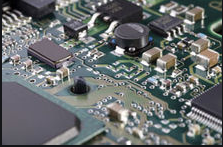
In pcba processing, when the surface tension of the solder is destroyed, it will cause poor soldering of surface mount c...
Factors affecting PCBA processing and cleaningIn the PCBA patch processing plant, in order to make the cleaning of print...
в процессе обработки PCBA, бесконтактная печать используется для печати с гибкими шелковыми шаблонами, с тем чтобы предоставить необходимый промежуток времени...
The development direction of SMT placement machineWith the rapid development of SMT, not only the size of electronic com...
система обработки и передачи кристаллов SMT представляет собой механическую коготь для перехода металла на роликах. Она поддерживает...
The first inspection mechanism refers to an error-proof mechanism to prevent mass accidents. Before pcba mass production...
Технологический процесс использования печатной паяльной пасты при обработке SMT патчей выглядит следующим образом: подготовка перед печатью - настройка рабочих параметров печатной машины - печать паяльной пасты - проверка качества печати - очистка и отделка.
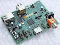
PCBA processability review.1. Selection of components. Solderability. Heat resistance. Coplanarity.In PCBA design, chip ...
Основные требования к сборке электронного оборудования PCBA для сборки и соединения электронного оборудования PCBA.
Pcba manufacturers have two pre-processing steps, lead forming and component insertion, before the components are solder...
PCBA Productive Design 1. оптимизация сборки на поверхности и сборки под давлением
Важным компонентом электронной продукции является PCBA. качество пайки PCBA напрямую зависит от...
технология PCBA имеет множество факторов, влияющих на мостик, таких, как дизайн, активность флюса, состав припоя, технология и т.д.
Ten principles for the use of chip inductance during Smt chip processing1. The spacing of the chip inductors should be s...
SMB design1. Component layoutThe layout is to arrange the components evenly and neatly on the PCB in accordance with the...
Таким образом, такая мелкая упаковка используется в большинстве небольших интегральных схем с менее крупными вводными проводами. есть несколько видов поэтому...
After the PCB board is soldered (including reflow soldering and wave soldering), light green bubbles will appear around ...