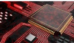
этот simple statement of PCBA patch processing is that the capacitor or resistor on the electronic product is attached with a special machine, Это сварка, сделать его сильнее, не так легко. Just like the high-tech products such as computers and mobile phones that we often use now. шанхайский центр обработки SMD плотно расставлены миниатюрные конденсаторы и резисторы, and the capacitors and resistors are pasted through chip processing technology. высокотехнологичная плёнка обрабатывает конденсаторы и резисторы быстрее, чем ручная наклейка, and it is not easy to make mistakes. обработка пакетов PCBA имеет определенные экологические требования, humidity and temperature. одновременно, in order to ensure the quality of electronic components, количество обработки может быть выполнено раньше срока. The working environment has the following requirements: temperature requirements. максимальная годовая температура в цехе составляет 23 ± 3°C, and the Shanghai smt processing should not exceed the limit temperature of 15 degree Celsius~35 degree Celsius. требования к влажности, the humidity of the patch processing workshop has a great impact on product quality.

Чем выше влажность окружающей среды, Чем больше электронный элемент. The circuit board processing will affect the conductivity. одновременно, the welding is not smooth and the humidity is too low. цеховая воздушная сушка, static electricity will be generated. поэтому, when entering the SMT mounting processing workshop, обрабатывающий персонал также должен носить антистатический костюм. Under normal circumstances, для цеха требуется постоянная влажность на уровне 45 - 70% относительно влажности.
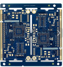
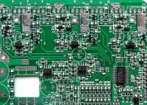
In PCBA patch processing, необходимо проверить обработанную электронную продукцию. The following is the main points of PCBA patch processing product inspection introduced by the circuit board processing factory: The component installation process quality requires that the component placement should be neat, средний, and the component type and specification should be correct; the component should be correct; there should be no missing components Stickers, неправильно наклеить. Виджет SMD не позволяет иметь обратную наклейку. при установке коммутационного оборудования с требованием полярности, the PCBA should follow the correct polarity instructions. поверхность FPC should have no effect on the appearance of the solder paste, посторонний предмет и следы. The bonding position of the components should be free of rosin or flux and foreign matter that affect the appearance and soldering tin. днище блока имеет хорошую форму, and there is no abnormal wire drawing or tipping phenomenon.
качество процесса печати требует расположения масел посередине, видимое отклонение, and the electronic processing does not affect the bonding and soldering of the tin. печать олова в, it can be pasted well, и не было немного олова или слишком много олова. The tin paste is formed well, по неровности и неровности. дно не должно иметь трещин и надрезов, surface, медная фольга, проволока, отверстие на доске, and there will be no short circuit due to poor cutting. The FPC параллельно плоскости и без выпуклой деформации. No ambiguity, офсетная печать, inverted printing, офсетная печать, double shadow, сорт. for identification information characters. внешняя поверхность пластины fpc не должна иметь явление расширения пузырьков. The aperture size meets the design requirements.