Placing the decoupling capacitor directly in the IC package can effectively control EMI and improve the integrity of the signal. This article starts with the internal packaging of the IC, analyzes the source of EMI and the role of IC packaging in EMI control, and then proposes 11 effective EMI control Design rules, including package selection, pin structure considerations, output drivers and decoupling capacitor design methods, etc., help design engineers choose the most appropriate integrated circuit chip in a new design to achieve the best EMI suppression performance. Existing system-level EMI control technologies include:
(1) The circuit is enclosed in a Faraday box (note thв mechanical package containing the circuit should be sealed) to achieve EMI shielding;
(2) Filtering and attenuation technology is adopted on the circuit board or the I/O port of the system to achieve EMI control;
(3) Strictly shield the electric field and magnetic field of the current circuit, or adopt appropriate design techniques on the circuit board to strictly control the capacitance and inductance of печатная плата traces and circuit board layers (self-shielding), thereby improving EMI performance.
EMI control usually requires a combination of the above-mentioned technologies. Generally speaking, the closer to the EMI source, the smaller the cost required to achieve EMI control. The integrated circuit chip on the печатная плата is the most important energy source of EMI. поэтому, if you can understand the internal characteristics of the integrated circuit chip in depth, you can simplify the EMI control in the печатная плата and system-level design.
печатная плата board-level and system-level design engineers usually believe that the EMI source they can reach is the печатная плата. Obviously, at the печатная плата design level, a lot of work can indeed be done to improve EMI. However, when considering EMI control, design engineers should first consider the choice of IC chip. Certain characteristics of integrated circuits, such as package type, bias voltage, and chip process technology (such as CMOS, ECL, TTL), etc., have a great influence on electromagnetic interference. В настоящем документе основное внимание будет уделено этим вопросам и обсуждению влияния IC на управление EMI.
1. The source of EMI
During the transition of digital integrated circuits from logic high to logic low or from logic low to logic high, the frequency of the square wave signal generated at the output is not the only frequency component that causes EMI. The square wave contains sinusoidal harmonic components with a wide frequency range, and these sinusoidal harmonic components constitute the EMI frequency components that engineers care about. The highest EMI frequency is also called the EMI emission bandwidth, and it is a function of the signal rise time rather than the signal frequency. The formula for calculating the EMI emission bandwidth is: F=0.35/Tr
Among them: F is the frequency in GHz; Tr is the signal rise time or fall time in ns (nanoseconds).
Из вышеприведенной формулы нетрудно понять, если частота переключения цепи составляет 50 МГц, время нарастания используемого чипа ис составляет 1 НС, then the highest EMI emission frequency of the circuit will reach 350MHz, which is much greater than the switching frequency of the circuit. And if the rise time of the IC is 500ps, then the highest EMI emission frequency of the circuit will be as high as 700MHz. Как известно, every voltage value in the circuit corresponds to a certain current, and also every current has a corresponding voltage. When the output of the IC changes from logic high to logic low or logic low to logic high, these signal voltages and signal currents will generate electric and magnetic fields, and the highest frequency of these electric and magnetic fields is the emission bandwidth. The strength of the electric and magnetic fields and the percentage of external radiation are not only a function of the signal rise time, but also depend on the control of the capacitance and inductance on the signal path between the signal source and the load point. Here, the signal source is located on the печатная плата интегральная схема внутри платы, and the load is inside other ICs. These ICs may or may not be on the печатная плата. In order to effectively control EMI, it is not only necessary to pay attention to the capacitance and inductance of the IC chip itself, but also to the capacitance and inductance existing on the печатная плата.
емкость цепи уменьшается, если связь между напряжением сигнала и сигнальным контуром не тесно, и поэтому подавляет электрическое поле, увеличивая тем самым EMI; то же самое происходит и с током в цепи, и если плохая связь между током одного и того же контура неизбежно увеличит индуктивность контура, тем самым укрепит магнитное поле, что в конечном счете приведет к увеличению Эми. Иными словами, неправильное регулирование электрического поля обычно приводит к неэффективному подавлению магнитного поля. Меры по регулированию электромагнитного поля в платы обычно аналогичны мерам, используемым для подавления электромагнитного поля в корпусе IC. как и при проектировании печатная плата, дизайн герметизации IC окажет огромное влияние на EMI.
A considerable part of the electromagnetic radiation in the circuit is caused by voltage transients in the power bus. When the output stage of the IC jumps and drives the connected печатная плата логическая линия "высокая", the IC chip will absorb current from the power supply and provide the energy required by the output stage. For the ultra-high frequency current generated by the continuous conversion of the IC, the power bus starts from the decoupling network on the печатная плата and ends at the output stage of the IC. If the signal rise time of the output stage is 1.0ns, then the IC must draw enough current from the power supply to drive the transmission line on the печатная плата in a short time of 1.0ns. The voltage transient on the power bus depends on the inductance in the power bus path, the current absorbed, and the transit time of the current. The voltage transient is defined by the following formula: V=Ldi/dt,
Among them: L is the value of the inductance on the current transmission path; di represents the current change in the signal rise time interval; dt represents the current transmission time (the rise time of the signal).
Since the IC pins and internal circuits are part of the power bus, and the rise time of the absorbed current and the output signal depends to a certain extent on the process technology of the IC, the above formula can be controlled to a large extent by choosing the appropriate IC. All three elements mentioned in.

2.IC роль упаковки в управлении электромагнитными помехами
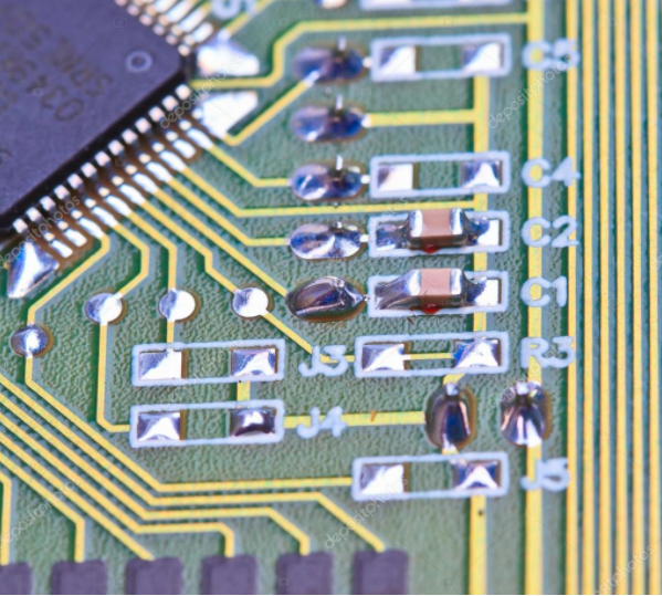
IC packages usually include: silicon-based chips, a small internal печатная плата, and pads. The silicon-based chip is mounted on a small печатная плата, and the connection between the silicon-based chip and the pad is realized through a bonding wire, and a direct connection can also be realized in some packages. маленький печатная плата realizes the connection between the signal and power supply on the silicon-based chip and the corresponding pins on the IC package, thus realizing the external extension of the signal and power supply nodes on the silicon-based chip. The power and signal transmission paths that penetrate the IC include: silicon-based chips, connections with small печатная платаs, печатная плата traces, and input and output pins of the IC package. The control of capacitance and inductance (corresponding to electric field and magnetic field) depends largely on the design of the entire transmission path. Некоторые проектные характеристики будут непосредственно влиять на емкость и индуктивность всей чип IC.
First look at the connection between the silicon-based chip and the internal small circuit board. Many IC chips use bonding wires to realize the connection between the silicon-based chip and the internal small circuit board, which is a very thin flying wire between the silicon-based chip and the internal small circuit board. This technology is widely used because the coefficient of thermal expansion (CTE) of the silicon-based chip and the internal small circuit board are similar. The chip itself is a silicon-based device, and its thermal expansion coefficient is very different from that of typical печатная плата materials (such as epoxy resin). Если электрическая точка подключения кристалла на основе кремния установлена непосредственно на внутренней микросхеме печатная плата, затем через относительно короткий период, внутренняя температура упаковки IC может привести к тепловому расширению и сужению, and the connection in this way will fail due to fracture . The binding wire is a lead method that adapts to this special environment. It can withstand a large amount of bending and deformation and is not easy to break.
The problem with using bonding wires is that the increase in the current loop area of each signal or power line will cause the inductance value to increase. A good design to obtain a lower inductance value is to achieve a direct connection between the silicon-based chip and the internal печатная плата, that is, the connection point of the silicon-based chip is directly bonded to the печатная плата pad. This requires the use of a special печатная плата board base material, which should have a very low CTE. The choice of this material will lead to an increase in the overall cost of the IC chip. Therefore, the chip using this process technology is not common, but as long as the IC that directly connects the silicon-based chip with the carrier печатная плата exists and is feasible in the design scheme, then Using such IC devices is a better choice.
Generally speaking, in the IC package design, reducing the inductance and increasing the capacitance between the signal and the corresponding circuit or between the power supply and the ground are the first choices for the process of selecting an integrated circuit chip. For example, small-pitch surface mount technology should be compared with large-pitch surface mount technology. IC chips packaged with small-pitch surface mount technology should be selected first, and these two types of surface mount technology package IC chips are better than via lead type packages. BGA packaged IC chips have the lowest lead inductance compared to any commonly used package types. From the point of view of capacitance and inductance control, smaller packages and finer pitches usually always represent improved performance.
An important feature of the lead structure design is the allocation of pins. Потому что значение индуктивности и емкости зависит от близости сигнала или источника к контуру, enough return paths must be considered.
Power and ground pins should be allocated in pairs, and each power pin should have a corresponding ground pin adjacent to each other, and multiple power and ground pin pairs should be allocated in this lead structure. Both of these features will greatly reduce the loop inductance between the power supply and the ground, and help reduce voltage transients on the power bus, thereby reducing EMI. по привычным причинам, many IC chips on the market now do not completely follow the above design rules. However, IC designers and manufacturers have a deep understanding of the advantages of this design method, so IC manufacturers are more inclined to design and release new IC chips. обратите внимание на подключение.
Ideally, assign an adjacent signal return pin (such as a ground pin) to each signal pin. The actual situation is not the case, Даже самые передовые производители IC так и не распределили фишки IC, but adopted other compromise methods. в пакете BGA, an effective design method is to set a signal return pin at the center of each group of eight signal pins. In this pin arrangement, each signal is between each signal and the signal return path. The difference is only one pin. For quad flat package (QFP) or other gull wing type ICs, it is unrealistic to place a signal return path in the center of the signal group. Even so, Необходимо обеспечить, чтобы каждый 4 - 6 штырей располагал сигналом обратного вывода. It should be noted that different IC process technologies may use different signal return voltages. Some ICs use ground pins (such as TTL devices) as the signal return path, while some ICs use power pins (such as most ECL devices)