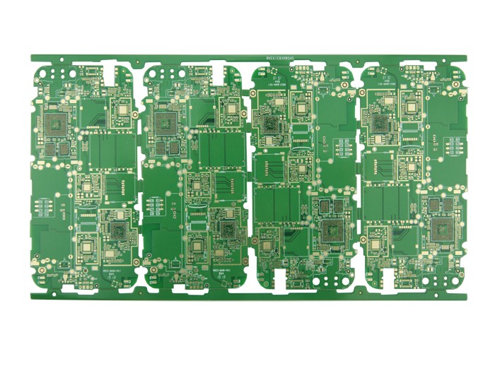
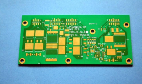
поговорить о сопротивлении многослойная плата
* Да * Нет * многослойная плата, почему многослойная плата Нужно ли полное сопротивление? Что такое импеданс и его тип, then it introduces why многослойная плата need impedance, and finally explains the meaning of impedance to PCB многослойная плата. следовать за редактором и узнать больше.
In a circuit with resistance, индуктивность, and capacitance, сопротивление переменного тока. Impedance is often represented by Z, Это множественное число. The real part is called resistance, номинальный реактанс. сопротивление емкости переменному току в цепи называется емкостным реактансом, and the hindering effect of inductance on alternating current in the circuit is called For inductive reactance, блокирующее воздействие емкости и индуктивности на переменный ток в схеме называется реактивностью. The unit of impedance is ohms.
(1) Characteristic impedance
In electronic information products such as computers and wireless communications, the energy transmitted by the circuit board in the circuit is a square wave signal (square wave signal, called pulse) composed of voltage and time, характеристическое сопротивление.
(2) Odd Mode Impedance
The impedance value of one line to the ground of the two lines is the same as the impedance value of the two lines.
(3) Even mode impedance
The two same signal waveforms with the same polarity are input to the drive terminal, сопротивление Zcom при соединении двух проводов.
(4) Differential impedance
Two identical signal waveforms with opposite polarities are input at the driving end, передача по двум разностным линиям, вычитание двух разностных сигналов в конце приёма. The differential impedance is the impedance Zdiff between the two wires.
(5) Common mode impedance
The impedance Zoe of one line to the ground of the two lines, величина сопротивления двух линий равна, usually larger than the odd mode impedance.
полное сопротивление многослойной платы означает параметр сопротивления и реактивности, which hinder the alternating current. в производстве плата цепи pcb, важность обработки импедансов. The reasons are as follows:

1. For multi-layer circuit boards (bottom of the board), consider plugging and installing electronic components. После заглушки, consider issues such as electrical conductivity and signal transmission performance. поэтому, the lower the impedance, лучше, and the resistivity should be less than 1 per square centimeter.&TImes ; Below 10-6.
2. процесс производства многослойных плат должен проходить через процесс погружения меди, tin electroplating (or chemical plating, or thermal spray tin), connector soldering, сорт., материалы, используемые в этих звеньях, должны обеспечивать низкий удельный сопротивление, чтобы обеспечить полное сопротивление платы, чтобы удовлетворить требования качества продукции и нормально работать.
- 3.... The tinning of многослойная плата Это самая легкая проблема в производстве всей платы., Это ключ к сопротивлению. The biggest defect of the electroless tin coating is easy discoloration (easy to be oxidized or deliquescent) and poor solderability, which will lead to difficult soldering of the circuit board, полное сопротивление, poor electrical conductivity, или неустойчивость общего функционирования Совета директоров.
4. There will be various signal transmissions in the conductors of the multilayer circuit board. когда необходимо увеличить частоту для повышения скорости передачи, из - за таких факторов, как травление, сама цепь будет приводить к импедансу, толщина слоистой пластины, and wire width. Это изменение вызовет искажение сигнала и снижает свойства платы. поэтому, it is necessary to control the impedance value within a certain range.
электронная промышленность, according to industry surveys, the most fatal weakness of the electroless tin coating is its easy discoloration (easy to be oxidized or deliquescent), из - за плохой сварки, and high impedance leading to poor electrical conductivity or instability of the overall board performance. Это может привести к короткому замыканию цепи PCB, даже к сжиганию или возгоранию.
It is reported that the first domestic research on chemical tin plating was Kunming University of Science and Technology in the early 1990s, followed by Guangzhou Tongqian Chemical (enterprise) in the late 1990s. Up to now, промышленность признала, что эти два органа являются лучшими. Among them, По нашим контактам, Многие компании экспериментальное наблюдение и долгосрочные испытания на выносливость, олово, подтверждаемое до прохода в химическую промышленность, является чистым оловянным слоем с низким удельным сопротивлением, электропроводность и качество пайки обеспечивают высокий уровень. No wonder they dare to guarantee to the outside that the coating can keep its color for one year, без пузырьков, без шелухи, and permanent tin whisker without any sealing and anti-tarnish protection.
потом, when the entire social production industry developed to a certain extent, Многие последующие участники часто повторяют друг друга. На самом деле, a considerable number of companies themselves did not have the R&D or initiative capabilities themselves. поэтому, many products and their users electronic products (circuit boards) The bottom of the board or the overall electronic product) performance is poor, А главная причина плохой работы - проблема импедансов., because when the unqualified electroless tin plating technology is in use, Она была покрыта многослойной схемой PCB. Tin is not really pure tin (or pure metal element), but a compound of tin (that is, Он вовсе не металлический элемент, but a metal compound, окись или галоид, or more directly, it is a non-metal substance) Or a mixture of tin compound and tin metal element, но найти его невооруженным глазом...
Because the main circuit of the multi-layer circuit board is copper foil, припой из медной фольги луженый, and the electronic components are soldered on the tin-plated layer through solder paste (or solder wire). In fact, the solder paste is melting. The molten state soldered between the electronic component and the tin plating layer is metal tin (that is, the metal element with good conductivity), Таким образом, можно просто сказать, что электронный элемент соединяется в медную фольгу на дне платы через луженое покрытие., so tin The purity of the coating and its impedance are the key; but before the electronic components are plugged in, когда мы непосредственно используем прибор для определения импеданса, in fact, the two ends of the instrument probe (or called the test lead) first touch the copper on the bottom of the панель PCB. затем соединяйте слой олова с поверхностью фольги в медную фольгу внизу платы для передачи тока. поэтому, tin plating is the key, ключ, влияющий на сопротивление и влияющий на характеристики всей платы, and it is also the key that is easy to be ignored.
Как известно, except for the simple substance of metal, its compounds are poor electrical conductors or even non-conductive (also, this is the key to the distribution capacity or spreading capacity in the circuit), Таким образом, при соединениях или смесях олова в луженом слое присутствуют квазиэлектропроводность, а не электропроводность, the existing resistivity or the resistivity after the electrolysis reaction due to future oxidation or damp and the corresponding impedance are quite high (enough to affect the level or signal transmission in the digital circuit) and The characteristic impedance is also not consistent. So it will affect the performance of the circuit board and the whole machine.
Therefore, as far as the current social production phenomenon is concerned, материал и свойства покрытия внизу платы являются наиболее важной и непосредственной причиной, влияющей на сопротивление характеристики всей платы. Потому что его изменчивость, the worrying impact of its impedance has become more invisible and variable. его скрытность объясняется главным образом:, it cannot be seen by the naked eye (including its changes), Следующий, it cannot be measured constantly because of its concealment. изменчивость с течением времени и влажностью окружающей среды, Так что это всегда легко игнорировать.