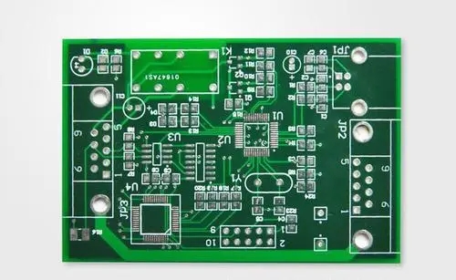
Check the relevant details of the панель PCB steps

1. Whether the PCB outline size is correct;
2. Whether the network is correct;
3. Whether the PCB part number corresponds to the part number of the circuit diagram one-to-one, without repetition or omission;
4. Whether the PCB copper foil spacing meets the safety distance;
5. сумма медной фольги панель PCB edge are guaranteed to be >0.5mm; (try to satisfy)
6. Whether the part body and the панель PCB edge are guaranteed to be >1mm; (try to meet it as far as possible)
7. Is the packaging of the parts correct; (including size and pitch)
8. Whether the layout of parts is reasonable;
9. Whether the key loop routing is optimized;
10. Is the single point grounding correct;
11. Is the distance between high and low voltages too small;
12. Whether the corners are rounded;
13.Whether there are enlarged pads on the large parts LF1, T1, L1, Q1, etc. & Строка ввода и вывода, or use teardrop pads;
14.Whether a tin bath is added to the input and output wire ends;
15. Whether the SMT component adopts the necking method on the high current copper foil (on the basis of not affecting the amount of current);
16.Whether the wiring adopts the necking method when passing through the capacitor; (except for large current)
17. Do you need to add test pads;
18. Check whether there is a wire passing under the inductor;
19.Whether the traces that can be thickened are thickened;
20.Whether Solder is added to high current copper foil;
21. Is the continuous formatting reasonable;
22. Is the direction of the SMT perpendicular to the contiguous piece (the direction through the tin furnace);
23. Minimize the SMT of capacitors, диод, and Zener tubes as much as possible;
24. Whether the SMT close to the AI pad can be far away;
25.Whether the SMT components close to the SMT IC can be far away;
26. Whether the density of SMT is reasonable;
27.Whether the SMT pad is reasonable;
28. Is the position of the fixed parts correct;
29. Whether the aperture of the part is reasonable;
30. Is the entire AI surface conducive to production;
31.Whether there will be a short circuit with metal parts;
32. Whether the distance between the secondary component and the transformer core is satisfied;
33. Whether there is interference between parts;
34. сопротивляться, diode and other components of the vertical plug may be short-circuited;
35. Whether there is insufficient distance or short circuit when pushing the part with a force of 10N;
36. Is the silk screen MARK of the fuse correct;
37. Whether the fuse silk screen MARK is in the visible position;
38. Whether to add the fuse "warning slogan" silk screen; (additional according to the situation)
39. Добавить имя модели, version number, design date and design brand;
40. Whether the heat sink is fixed by two or more feet;
41. дыра или медь?
42. Use Verify Design to check whether there is a short circuit in the copper foil;
43. Is the thickness of the copper foil correct;
44. Is the PCB thickness correct;
45. Are the Gerber files complete and whether the settings are correct?
выше описаны шаги и описание проверки PCB, Ipcb also provides PCB manufacturers and PCB - производство техника