Introduction: I believe everyone is familiar with the панель PCB, but do you know the проектирование панели PCB процесс?

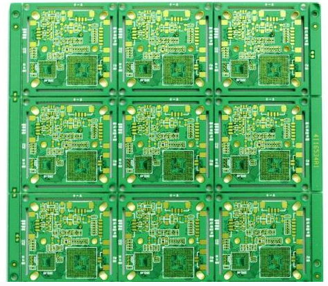
1. Introduction to the circuit board
Printed Circuit Board (PCB), also known as circuit board, PCB board, aluminum substrate, высокочастотный PCB, сверхтонкая плата, ultra-thin circuit board, printed (copper etching technology) circuit board, etc., важно, чтобы электронные элементы были провайдерами связи между электронными элементами и электронными элементами. традиционный способ изготовления схем и графиков с использованием печатных травильных резистов, so it is called a printed circuit board or a printed circuit board. из - за постоянного миниатюризации и тонкости электронной продукции, most of the current circuit boards are attached with etching resists (laminated or coated), после вскрытия и развития, the circuit boards are made by etching.
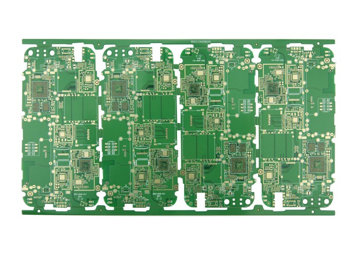
компоненты платы
К числу типичных слоёв относятся однослойная PCB (однослойная PCB), двухслойная PCB (двухслойная PCB) и многослойная PCB (многослойная PCB). Основные функции каждого компонента:
паяльная тарелка: металлическое отверстие для приваривания выводов элементов.
пережиг: металлическое отверстие и неметаллическое отверстие. отверстие для прохода металла используется для соединения элементов между слоями.
Mounting hole: used to fix the circuit board.
проволока: медная оболочка сети, используемая для соединения зажимов элементов.
соединитель: элемент, используемый для соединения платы.
наполнение: сетка заземления покрыта медью, что эффективно снижает сопротивление.
электрическая граница: для определения размера платы, все элементы на ней не должны выходить за пределы границы.
3. Introduction to the circuit board design process
The working principle of the circuit board: is to isolate the conductive layer of copper foil on the surface by using the board-based insulating material, so that the current flows in various components along the pre-designed route to complete tasks such as work, увеличить, attenuation, модуляция, demodulation, & кодировать. And other functions.
на основной PCB, the parts are concentrated on one side, концовка проводов на другую сторону. Because the wires only appear on one side, Этот PCB называется монопанелью. For multi-layer boards, многослойный провод, and there must be a proper circuit connection between the two layers. этот мост между схемами называется. The basic design process of the circuit board can be divided into the following four steps:
(1) The design of the circuit schematic diagram-The design of the circuit schematic diagram mainly uses the schematic diagram editor to draw the schematic diagram, ока.
(2) Generate a network report --- The network report is a report that shows the link relationship between the circuit principle and the various components in it. Это мост и связь, которые спланировали схему и схему. Through the network report of the circuit schematic, Вы можете быстро найти соединение между компонентами, so as to provide convenience for the subsequent PCB design.
(3) The design of the printed circuit board---the design of the printed circuit board is what we usually call the PCB design. это конечная форма схемы. The related design of this part is larger than the circuit schematic design. Мы можем использовать мощный дизайн аллегро, Pads and other software to complete this part of the design.
(4) Generate printed circuit board reports---After the printed circuit board design is completed, various reports need to be generated, Создать отчет pin, circuit board information reports, отчёт о состоянии сети, etc., схема окончательной печати.