There was no special схема PCB перед, especially for mobile phones. сначала, I felt that there was nothing, но в конце концов, Я совсем свихнулся.. There is no way out. истинный! The boss started talking about 6 days. начать с компоновки, I wonder if the boss is crazy. Некоторые коллеги на самом деле говорят да! Я очень хочу резать людей кухонным ножом. Later, Босс сказал: "немного туго, or else, делать вдвоём. I rely on, босс очень творческий. There is no way to call me a part-time job. Вот так, моя самая болезненная и долгосрочная планировка PCB началась. In addition, несколько дней назад было 6 недель без отдыха., and now itâs fine. вечером на работе прохладно! Cool!

Теперь я действительно не хочу жить!
Не говори, что ты делаешь лучше, чем плохо., Даже если не удалось.
Stop talking nonsense, Позвольте мне начать с моего опыта.. If there are professionals, здесь специалист или старший инженер, please give us more opinions and suggestions!
Я использую питание PCB 5.0.
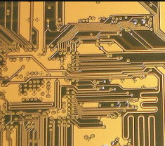
1. The thread ends first
2. Tightly trace
3. верхняя и нижняя провода должны быть как можно более перекрыты, leaving room for punching holes
4. не заграждать дорогу при проводке, give the surrounding space as much as possible
5. The punching area and wiring area can be separated
6. Кроме GND, убывающее отверстие.
7. Less wiring in the lower layer of the IC
8. To be proficient in the use of tools, functions and quick decision keys
9. Do not run wires on the holes
10. В случае необходимости, holes can be punched on the BGA pads
11. компоновка очень важна, analyze the density and direction of the flying line (the principle of proximity)
12. You can go close to the peripheral devices first (if there is a flying line, Вы можете ходить по внешнему устройству, and try to make as little as possible)
13. если есть несколько подключений, look wherever is near and convenient, then go where
14. After punching under the IC, it is best to walk closer to the IC boundary
15. Try to go to the surface as far as possible in the short-term.
16. When wiring, Соответствующая схема, it is best to print it out
17. Во - первых, наберите ближе к IC на поверхности, Так ты сможешь пробить дыру там. (No worries)
18. время размещения, the ones that can be placed closer must be placed closer, особенно в отношении BGA, the layout is the first, режим является вторым, and the beauty is third.
19. Wiring is a systematic task, лучше сделать один, if there is more than one, Это может привести к смерти.
20. если вы сможете спланировать корзину, you must consider the margin and strive for space.
21. When making the schematic diagram, Он должен быть лаконичным и четким, with fewer components, высокая степень интеграции, and sealed, маленький, optional components must be removed.
22. Distinguish which lines are set or settable (there is no other way to move) should go first, перемещать в будущем.
23. если возможно, leave the trace width between devices during layout.
24. Three-dimensional lines should be used for large-scale BGA ICs (multi-layers). Do not use flat surfaces (all on the same layer). You will know what it means later.
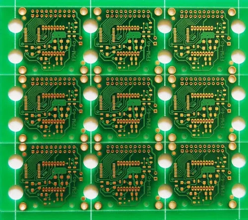
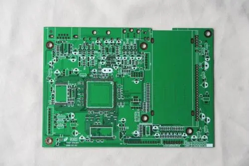
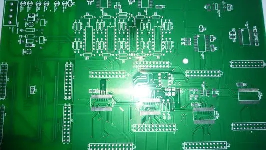
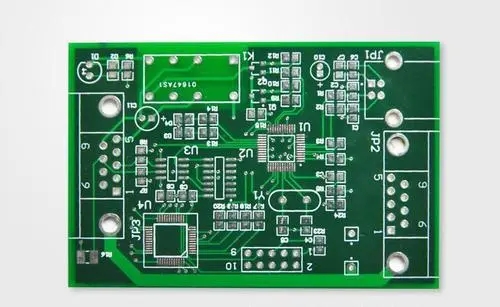
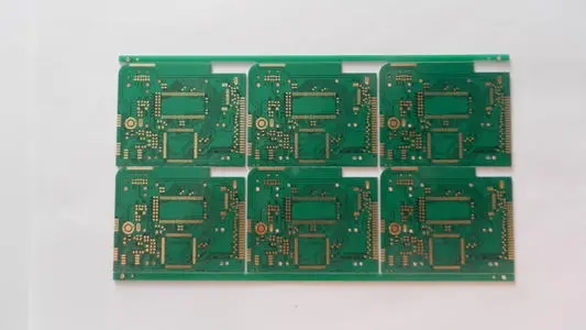
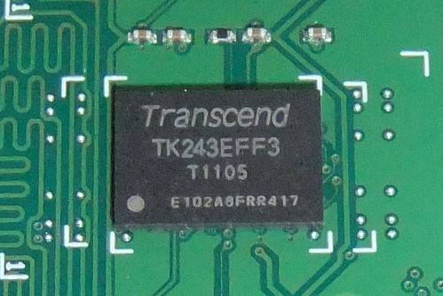
это описание мобильного телефона. рисунок PCB опыт, Ipcb также предоставляет Производители PCB and PCB manufacturing technology.