PCB process design specification 2
Screen printing requirements for технологическое проектирование PCB
All components, монтажное отверстие, установочное отверстие с соответствующей меткой
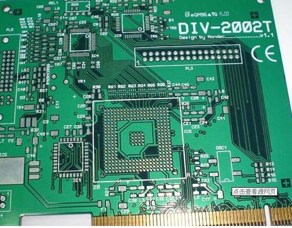
In order to facilitate the installation of the board, все компоненты, mounting holes, and positioning holes have corresponding silk-screen marks.
The mounting hole silk screen is marked with H1, H2...Hn.
Silk screen characters follow the principle of from left to right and from bottom to top
The silk screen characters should follow the principle of from left to right and bottom to top as far as possible. For devices with polarities such as electrolytic capacitors and diodes,
Попробуйте сохранять одно и то же направление в каждой функциональной единице.

There is no silk screen on the device pad and the tin track that needs to be tinned, после установки номер устройства не должен быть экранирован устройством. (Higher density,
There is no need to remove the silk screen on the PCB)
In order to ensure the soldering reliability of the device, it is required that there is no silk screen on the device pad; in order to ensure the continuity of the tin channel, it is necessary to
There is no silk screen on the tin track that needs to be tinned; in order to facilitate the device insertion and maintenance, the device tag should not be covered by the device after installation
Block; the silk screen can not be pressed on the vias and pads, во избежание потери частичных шелковых сеток при открытии сварной маски, which will affect the training. Silk
Print spacing is greater than 5mil.
The polarity of polarized components is clearly indicated on the silk screen, метка направленности поляризации.
The direction of the directional connector is clearly indicated on the silk screen.
There should be a barcode location mark on the PCB
When the панель PCB пространственное разрешение, there should be a 42*6 barcode silk screen frame on the PCB, and the position of the barcode should be considered
It is easy to scan.
панель PCB name, дата, version number and other information screen printing position should be clear.
файл PCB должен распечатать имя платы, date, номер версии и другая информация, and the position is clear and eye-catching.
на печатных платах должна быть полная информация изготовителя и антистатические знаки.
The number of PCB light drawing files is correct, на каждом этаже должен быть правильный вывод, and there should be a complete output of the number of layers.
идентификатор устройства на PCB должен соответствовать идентификатору в таблице BOM.
Safety requirements
The safety mark of the insurance tube is complete
Are there 6 complete marks near the fuse, включать номер последовательности предохранителей, fusing characteristics, номинальное значение тока, explosion-proof special
Characteristic, номинальное напряжение, English warning label.
например F101 F3.15 а, 250Vac, "Внимание: для предотвращения риска пожара на постоянной основе,
Replace Only With Same Type and Rating of Fuse".
предупреждать по - английски, если нет места на PCB, you can put the labor and English warning signs in the product manual
illustrate.
Hazardous voltage areas on the PCB are marked with high-voltage warning symbols
The dangerous voltage area of the PCB should be separated from the safe voltage area by a 40mil-wide dashed line, маркировка риска высокого давления.
идентификация и "опасность"! HIGH VOTAGE".
The original and secondary side isolation belts are clearly marked
The original and secondary side isolation strips of the PCB are clear, and there is a dotted line mark in the middle.
панель PCB safety signs should be clear
Five safety signs for панель PCB (UL certification mark, изготовитель, manufacturer model, номер файла аутентификации UL, flame retardant grade)
complete.
Reinforced insulation and isolation belt electrical clearance and creepage distance meet the requirements
The electrical clearance and creepage distance of the reinforced insulation isolation belt on the PCB meet the requirements. требования к конкретным параметрам, please refer to the relevant "PCB Safety Design Specification for Information Technology Equipment".
устройство, зависящее от изоляционной ленты, все еще должно удовлетворять вышеуказанным требованиям при тяге 10N.
Except for the effective basic insulation from the shell to the pin of the safety capacitor, the shells of other devices are not considered to have
Effective insulation, certified insulation sleeves and tapes are considered effective insulation.
Basic insulation isolation belt electric clearance and creepage distance meet the requirements
The safety distance between the shell of the primary device and the grounded shell meets the requirements.
The safety distance between the shell of the primary device and the grounding screw meets the requirements.
безопасное расстояние между оболочкой первичной установки и заземленным радиатором соответствует требованиям. (The specific distance size is determined by looking up the table)
Cables made into boards to bridge dangerous and safe areas (original and secondary sides) shall meet the safety requirements of reinforced insulation
Considering the 10N thrust, the devices on both sides close to the transformer core should meet the requirements of reinforced insulation
Considering the 10N thrust, the device close to the floating metal conductor should meet the requirements of reinforced insulation
For multi-layer PCBs, the copper foils between the original and secondary sides of the inner layer should meet the requirements of the clearance creepage distance (the pollution level is according to the
Calculate according to 1.)
For multilayer PCBs, the distance (including inner layers) near the via holes should meet the requirements of electrical clearance and creepage distance
For the dielectric thickness of the primary side and the secondary side between the multilayer PCB layers, Эти требования являются частью § 0.4mm
The thickness between layers refers to the thickness of the medium (excluding the thickness of the copper foil), among which 2-3, 4 - 5, 6-7, 8,9, 10-11
The core board is used in the interlayer, препрег для других прослоек.
A minimum safety distance of 2mm must be ensured between the exposed welding terminals of different voltages. сварной зажим следует вставлять после сварки.
Tilting and tilting may occur, уменьшить расстояние.