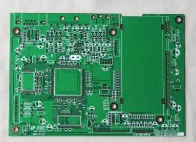
There are many ways to design jigsaw puzzles, В ходе опытного производства новой продукции иногда трудно определить, какой метод головоломки и количество мозаик. PCB design engineers give priority to meeting the structural requirements of the product during the design according to product characteristics (such as product structure limitation, ограничение высоты периферийного интерфейса, position limitation, сорт.), followed by feedback of sheet utilization и production during PCB manufacturing and SMT processing. The question of efficiency. Выберите PCB в процессе производства, the thermal expansion after encountering different geometric dimensions and PCB boarding methods directly affects the reliability and performance of the product, это увеличивает трудности обработки и себестоимость производства SMT. Combining the experience summaries of SMT process engineers for many years, повышение эффективности линии SMT, there are the following aspects to share with you:

· In the SMT production line, чтобы повысить коэффициент использования производственных линий, there are two common ways of splicing AAAA or AB. Мы не можем просто спросить? This should be considered from the complexity of the product process, балансировка цикла установки машины после сборки панелей, and the problem of parts drop after the second remelting of the bulky component, и так далее.
· The positive and negative design (AABB) has the advantage of making SMT production line equipment configuration and process simple and easy. опалубка, a set of patch procedures, Spi/AOI процедура проверки, and reflow soldering furnace temperature curve optimization once, сорт., to increase the speed of SMT rapid line change and complete the first piece verification at one time, and PCBA завершено products can be produced in a very short time Give out to the next process function test.
• недостатки в проектировании положительных и отрицательных полюсов (AABB) заключаются в том, что, если поверхность и верхняя поверхность продукта существенно отличаются друг от друга по компоновке компонентов (более крупная основная микросхема, более плотная компоновка элементов, более высокая плотность обратной связи через отверстие, чем ступни элемента, выходящие за поверхность платы), то это может привести к плохой и неустойчивой печати пасты в мелком пространстве; В ходе второй операции компоненты, имеющие большой объём и вес, рискуют потерять деталь. в массовом производстве не только не решаются вопросы повышения эффективности, но и возникают трудности с обработкой и качеством. Проблема в том, что это также экзамен на способность инженеров в онлайновом режиме изучать технику.
· Adopt (AAA/BBB) non-positive and negative design, какой больше подходит большинству заводов. The production line is easy to deploy and the equipment resources are rationally arranged. стабилизация производственного процесса, and it is easy to improve the efficiency of the production line. Когда? проектирование PCB, engineers must consider the rationality of the layout of the overall main chip components, большая тепловыделяющая сборка, and peripheral interface components. The processing plant only needs to reasonably arrange the production line to produce the BOT surface (less component surface) and then the TOP surface (multiple component surface). ), the process engineering is easier to deal with when the quality is abnormal during the processing.