Content preview:
1 Introduction
2. Signal integrity issues
3. Electromagnetic compatibility issues
4. Power integrity issues
5. General specification for high frequency circuit design
6. General specification for design of digital-analog hybrid circuit

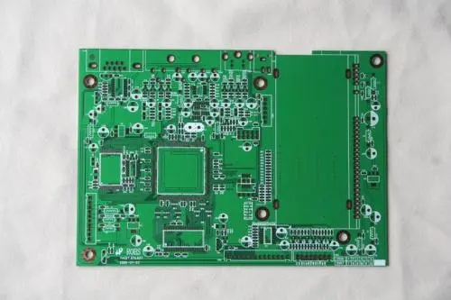
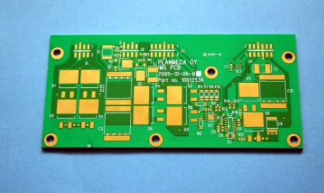
One: The definition of Hochfrequenz-Leiterplatte
*In digital circuits, Ob es sich um eine Hochfrequenzschaltung handelt, hängt von den steigenden und fallenden Kanten des Signals ab, nicht die Frequenz des Signals.
Formel: F2 =1/(Tr*Ï), Tr ist der Aufstieg/Fallverzögerung des Signals.
*F2> 100MHz, Es sollte in Übereinstimmung mit der Hochfrequenzschaltung betrachtet werden, the following conditions must be designed in accordance with the high-frequency rules
-The system clock frequency exceeds 50MHz
-Using devices with rise/fall times less than 5ns
--Digital/analog hybrid circuit
*Logic device rise/Sturzzeit und Verdrahtungslänge Anstieg/drop main harmonic spectrum distribution Maximum transmission line maximum transmission
Falling time Tr component F2=1/Fmax=10*distance (microstrip) line distance (microstrip line) ÏTr F2
74HC 13-15ns 24MHz 240 MHz 117cm 91cm
74LS 9.5ns 34 MHz 340MHz 85.5cm 66.5cm
74H 4-6ns 80 MHz 800MHz 35 28
74S 3-4ns 106 MHz 1.1GHz 27 21
74HCT 5-15ns 64 MHz 640MHz 45 34
74ALS 2-10ns 160 MHz 1.6GHz 18 13
74FCT 2-5ns 160 MHz 1.6GHz 18 13
74F 1.5ns 212 MHz 2.1GHz 12.5 10.5
ECL12K 1.5ns 212 MHz 2.1GHz 12.5 10.5
ECL100K 0.75ns 424 MHz 4.2GHz 6 5
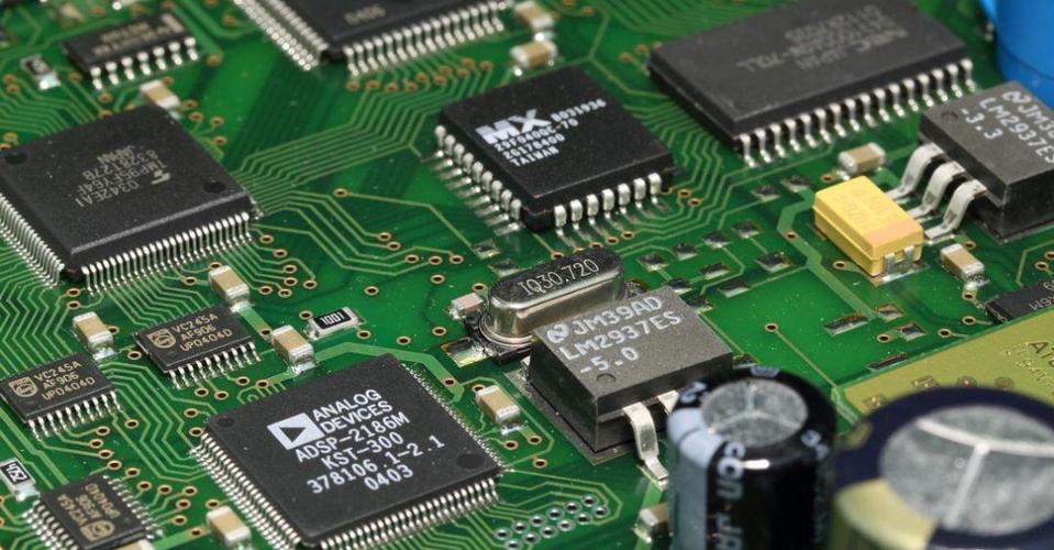
Traditional PCB-Designmethods are inefficient:
Schematic diagram, Traditionelle Entwurfsmethode Design und EingangsLayout und Verdrahtung haben keine Qualitätskontrollpunkte. Jeder Schritt von PCB-Design basiert auf Erfahrung. Wenn Probleme gefunden werden, sie/Sie müssen bei Null anfangen. Es ist sehr schwierig, Probleme in Funktions- und Leistungstests zu finden.
Signal integrity issues:
1. Reflection problem
2. Crosstalk issues
3. Overshoot and oscillation
4. Delay
Reflection problem: echo on the transmission line. Part of the signal power (voltage and current) is transmitted to the line and reaches the load, but there is a part
The points are reflected.
Multipoint reflection
Reason for reflection:
*Impedance mismatch between source and load
*The geometry of the wiring
*The direction of the wiring, via
*Incorrect wire termination
*Transmission through the connector
*Discontinuity of the power plane, etc.
Crosstalk issues:
*Crosstalk: Coupling between two signal lines
1. Capacitive crosstalk
*This happens when the lines are close to each other at a certain distance.
*Capacitive coupling induces coupling current
2. Inductive crosstalk
*Signal coupling between the primary coil and the secondary coil of the unneeded transformer
*Inductive coupling triggers coupling voltage.
Crosstalk issues:
The parameters of the Leiterplattenschicht, der Abstand der Signalleitungen, die elektrischen Eigenschaften des Antriebsenden und des Empfangsenden, und die Leitungsabschlussmethode haben alle einen bestimmten Einfluss auf das Übersprechen.
*The crosstalk of capacitance and inductance increases with the increase of load impedance, Daher sollten alle Leitungen, die für Übersprechen anfällig sind, mit Leitungsimpedanz beendet werden.
Methods to reduce capacitive crosstalk:
* Separating signal lines can reduce the energy of capacitive coupling between signal lines.
*Using the ground wire to separate the signal line can reduce the coupling of capacitance. Verbesserung der Wirksamkeit, Der Erdungskabel sollte jeden Tag mit dem Erdungskabel verbunden werden./4 Zoll. (Î wavelength refers to the distance the signal is transmitted per unit time.)
////////////////////////////
General principles:
Punch holes every 2-5cm.
Simulation results of capacitive crosstalk
=============
Ways to reduce perceptual crosstalk
*In order to solve the crosstalk problem of inductance, die Größe der Schleife sollte so weit wie möglich reduziert werden.
*By avoiding the situation that the signal return line shares a common path, Induktivitätsübersprechen, overshoot and oscillation can also be reduced
*Overshoot: Overshoot can cause false clocks or bus data read/Schreibfehler.
*Ringing: The phenomenon of ringing is repeated overshoot and undershoot.
Signaloszillation und Umgebungsoszillation werden durch übermäßige Induktivität und Kapazität auf der Leitung verursacht. Die Schwingung gehört zum unterdämpften Zustand und die umgebende Schwingung zum unterdämpften Zustand.
Oszillation kann durch ordnungsgemäße Beendigung reduziert werden, aber es ist unmöglich, es vollständig zu beseitigen.
Time delay: the different time delays of each signal line in a set of buses
Clock and signal: ensure as wide a window as possible
////////////////////////////
Electromagnetic compatibility issues
*Electromagnetic Interference (EMI) issues
1. Loop Design, forming antenna effect
2. The slot in the power layer will form a quarter-wavelength antenna
*Dense vias (such as BGA packaged devices)
*Large connectors (especially the backplane)
3. Induktive Komponenten.
Hinweis: Zwei parallele Induktivitäten auf der Bauteiloberfläche bilden einen Transformator.
Unreasonable return path leads to EMI
EMI caused by incomplete ground plane
Incomplete ground plane can cause large EMI
The simulation without considering the incomplete ground plane is inaccurate
////////////////////////////
Power integrity issues
*High-power high-speed devices: need a large transient current
*The ground layer and power layer are incomplete: 1. Split, über 2. Connector
*Filter capacitor: 3. Menge, Kapazität, layout,
Selection of power supply filter capacitor:
The system has both high frequency noise and low C0G (non-ferromagnetic) type frequency noise. Es ist höher als andere Arten durch Parallelisierung großer elektrischer 0.01μF Kondensatoren.
Kapazität, kleines ESL-Gerät, extrem klein 0.1μF Kondensator, ESL-Gerät kann den Filterbereich bei hoher Frequenz erweitern und hat eine bessere Filterleistung
////////////////////////////
Schematic design specification
Signal integrity and electromagnetic compatibility considerations
Correspondence between the schematic diagram and the PCB after the PCB is completed
General rules and requirements
*According to the unified requirements, Zeichnungsgröße auswählen, Rahmenformat, grafische Symbole und Textsymbole im Schaltplan.
* According to the electrical working principle of the product, Die Komponenten sollten in einer Reihe oder Reihe von rechts nach links und von oben nach unten angeordnet sein.
*When the drawing is arranged, Das Netzteilteil ist in der Regel unten links angeordnet, die Eingangsklemme befindet sich auf der rechten Seite, und der Ausgang ist auf der linken Seite.
*The working state of the movable components (such as relays) in the picture is in principle in the open and unpowered working position.
*Use all the power and ground pins of all chips.
////////////////////////////
Signal integrity and electromagnetic compatibility considerations
*Add corresponding filtering/absorption devices to the input and output signals; add silicon transient voltage absorption diode or varistor SVC if necessary
*String resistors on the high-frequency signal output terminal.
*The decoupling capacitors in the high frequency area should be electrolytic capacitors or tantalum capacitors with low ESR
*When determining the value of the decoupling capacitor, Wählen Sie einen Kondensator mit kleinerem Wert unter der Bedingung, dass die Ripple-Anforderungen erfüllt werden, um seine Resonanzfrequenz zu erhöhen.
* The power supply of each chip must be added with decoupling capacitors, und die Stromversorgung jedes Moduls in demselben Chip muss separat mit Entkopplungskondensatoren ergänzt werden; wenn es Hochfrequenz ist, eine magnetische Perle/Induktor muss zur Stromversorgung hinzugefügt werden.