13 things that CаM engineers should pay atдесятьtion to in проектирование PCB
The following contents are basically common to every PCB manufacturer, but they are not absolutely the same, разные поставщики.
раз. перекрытие земли

The overlap of pads (except surface mount pads), То есть, the overlapped placement of holes, при бурении скважин, из - за того, что в одном месте много отверстий, может привести к разрыву долота и повреждению проволоки.
два. Misuse of the graphics layer
1. нарушение обычного проектирования, such as component surface design on the BOTTOM layer and welding surface design on the TOP, Ошибка при редактировании файла на лицевой и обратной стороне файла.
2. If there are slots that need to be milled in the панель PCB, использовать запретный слой или панель для рисования их, do not apply other layers or fill them with pads to avoid mis-milling or miss-milling
3. если на двухсторонней пластине есть отверстия без металлизации, it should be stated separately.
три. Shaped hole
If there are irregular holes in the board, использовать запретный слой для рисования области заливки с размерами отверстий. The length/соотношение ширины фасонных отверстий должно быть 2: 3: 1, and the width should be >1mm. иначе, the drilling machine will easily break the tool when processing the special-shaped hole, это приведет к трудностям.
Four. Character placement
1. The characters cover the pad SMD soldering piece, Это неудобно для непрерывного испытания печатных плат и для приваривания элементов.
2. ролевой дизайн слишком мал, which makes the screen printing difficult and makes the characters not clear enough. высота знака - 30 мм, widthâ¥6mil.
пять. Single-sided pad aperture setting
1. односторонняя прокладка обычно не сверлилась. If the drilling needs to be marked, апертура должна быть спроектирована как нулевая. If the value is designed so that when the drilling data is generated, сверлить в таком положении, which will affect the appearance of the board, Совет директоров будет упразднен.
2. If the single-sided pad needs to be drilled, необходимо сделать специальную метку.
шесть. Draw pads with filling blocks
Drawing pads with filler blocks can pass the DRC inspection when designing the circuit, Но это не способствует переработке. поэтому, similar pads cannot directly generate solder mask data. при использовании ингибитора, the area of the filler block will be covered by the solder resist, вызывать затруднение сварки оборудования.
seven. There are too many filler blocks in the design or the filler blocks are filled with very thin lines
1. The light drawing data is lost, неполные данные светографа, and the light drawing is deformed.
2. Because the filling blocks are drawn one by one with lines during light drawing data processing, генерированный световой график, which increases the difficulty of data processing.
восемь. Surface mount device pad is too short
This is for continuity testing. установка для нанесения покрытия на поверхность с повышенной плотностью, the spacing between the two pins is quite small, и подушка тонка. The installation test must be staggered up and down (left and right), например, конструкция подушки слишком мала. Short, Хотя это не влияет на размещение оборудования, but it will make the test pin staggered.
девять. The spacing of the large area grid is too small
The edges between the same lines that make up the large-area grid are too small (less than 0.30mm), which will cause a short circuit during the printing process.
ten. The distance between the large area of copper foil and the outer frame is too close
The outer frame of the large area copper foil should be at least 0.перегородка 20 мм, because when milling the shape, Это легко приводит к короблению медной фольги, что приводит к отслоению флюса.
eleven. The design of the outline frame is not clear
Some customers have designed contour lines in KеEP LAYER, BOARD LAYER, верхний этаж, сорт. and these contour lines do not overlap, Это затрудняет определение в процессе формирования линии контура.
twelve. Line placement
The line between the two pads, do not draw intermittently, если вам нужна грубая линия, do not use the line to repeat the placement, Изменить ширину линии, so that it is easy to modify when modifying the line.
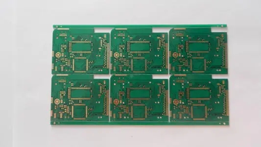
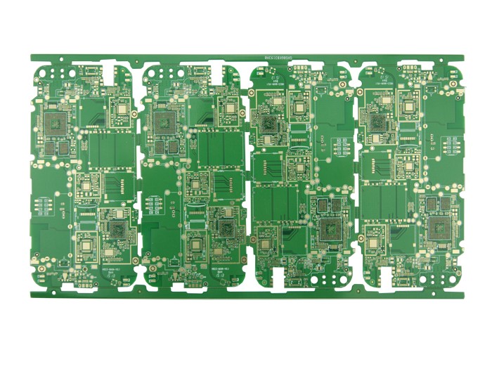
тринадцать. Imposition
The track system of the automatic welding equipment has a size range for clamping the панель PCB. The clamping range of the general production line is: 50mm*50mm-460mm*460mm. The small 50mm*50mm панель PCB needs to be designed into an imposition form.
A. PCB must have its own reference point (Mark) to facilitate the automatic location of welding equipment.
B. If the V-cut processing method is adopted, интервал между верстками должен быть 0.3mm, односторонний край технологии должен быть 5 мм.
C. PCB для сложных форм, после сборки PCB следует, насколько это возможно, обеспечивать правила формы, чтобы удерживать дорожку.
D. то же самое, что и PCB, and different PCBs can also be put together.
E. Imposition can be in the form of flat row, выстраивать, или мандаринка.

![Процесс проектирования PCB [turn] [PCB Technology]](/public/upload/image/20211101/02dcafe72b0ee319f6836d490bab9a17.jpg)