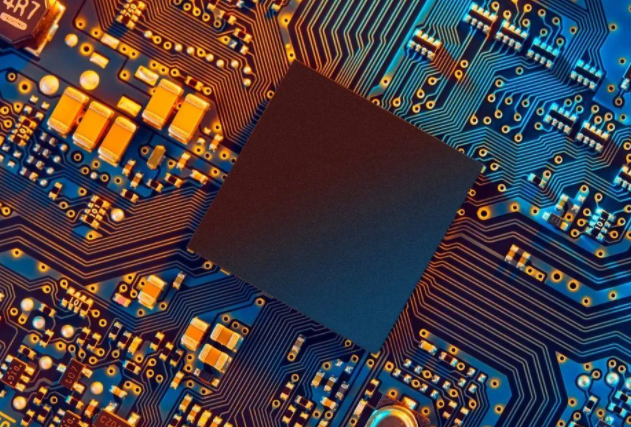
11 suggerimenti sul cablaggio del circuito ad alta frequenza
1. Le linee ad alta frequenza sono molto preoccupate per la corrispondenza e l'instradamento dell'impedenza. But if you can, si può fare esattamente lo stesso secondo il disegno di riferimento del produttore. After all, il progetto del costruttore è stato sottoposto a un calcolo più completo.
2. When you first draw ilPCB, please do not arrange your high-frequency traces according to the ordinary signal lines. It is the right way to obtain the reference design from the chip manufacturer. The general chip data manual or related manuals will have high-frequency parts. Il riferimento del cablaggio.
3. The entire high-frequency part can be dotted with more vias to increase ground connectivity. The ground copper has a great influence on the high-frequency wiring. Se non è correttamente instradato, the power supply or other signal lines will have 100k-300K interference signals.
4. Remember not to separate the ground, at least make sure that one side of the ground is a complete ground. Ensure that one side of the ground can be fully copper-clad, e non separarlo con linee di segnale.

5. Non posizionare un oscillatore di cristallo accanto a tracce ad alta frequenza. L'alta frequenza colpisce l'alta frequenza, questo è buon senso, cerca di tenerlo il più lontano possibile. Naturalmente, altre linee di segnale non dovrebbero essere troppo vicine alla linea ad alta frequenza, poiché l'alta frequenza influenza anche la bassa frequenza.
6. Posizionare vias accanto a tracce ad alta frequenza per migliorare efficacemente la qualità del segnale. The high frequency itself should need a shielding cover or shielding layer, ma il coperchio di schermatura non può essere fornito quando il circuito è instradato. At this time, thePCB itself can only be used to make a shielding layer. La via può essere intesa come lo strato di schermatura. The ground below is another layer. Quanto sopra potrebbe non essere in grado di aumentare la schermatura, because it needs to be exposed for debugging.
7. Whether it is the drawing of the schematic diagram or the design of the Scheda di copiaPCB, it should be considered from the high-frequency working environment in which it is located, per poter progettare un ideale più adattoPCB Copia scheda.
8. Almost every software has automatic layout, ma come unPCB engineer, si dovrebbe abbandonarlo e fare layout da soli per fare PCB production more effectively and reasonably.
9. Generalmente, i componenti della posizione fissa relativi alla dimensione meccanica sono posti prima, poi i componenti speciali e più grandi, e infine i componenti piccoli. Allo stesso tempo, è necessario tenere conto dei requisiti del cablaggio, il posizionamento dei componenti ad alta frequenza dovrebbe essere il più compatto possibile e il cablaggio delle linee di segnale può essere il più breve possibile, riducendo così l'interferenza incrociata delle linee di segnale.
10. The original is generally not too close to the edge, preferibilmente 3-5mm. Power sockets, interruttori, interfaces betweenPCB schede di copia, indicator lights, ecc. are all positioning plug-ins related to mechanical dimensions. Generalmente, the interface between the power supply and thePCB è posizionato sul bordo delPCB, and there should be a distance of 3mm to 5mm from the edge of thePCB; i diodi emettitori di luce devono essere posizionati accuratamente in base alle esigenze; interruttori e alcuni componenti di messa a punto, such as adjustable inductance, Resistenza di regolazione, ecc. dovrebbe essere posizionato vicino al bordo delPCB for easy adjustment and connection; components that need to be replaced frequently must be placed in a location with fewer components for easy replacement.
11. Whether the layout is reasonable or not directly affects the product's life, stabilità, EMC (electromagnetic compatibility), etc. It must be based on the overall layout of the circuit board, l'operatività del cablaggio e la fabbricabilità delScheda di copia PCB, struttura meccanica, and heat dissipation. , EMI (electromagnetic interference), reliability, l'integrità del segnale e altri aspetti sono presi in considerazione in modo esauriente.