Matters needing attention in high frequency circuit boards
Quando produciamo circuiti stampati ad alta frequenza, dovremmo prestare attenzione a quanto segue:
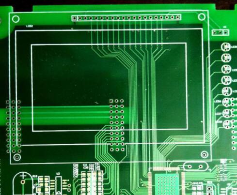
1) Reasonably choose the number of layers: When high-frequency circuit board wiring, use the middle inner plane as the potenza and ground layer, che può efficacemente ridurre l'induttanza parassitaria, shorten the length of signal lines, e ridurre le interferenze incrociate tra i segnali. Generally speaking, il rumore di una scheda a quattro strati è 20 dB inferiore a quello di una scheda a due strati.
2) Wiring method: In Progettazione PCB, durante il cablaggio di circuiti stampati ad alta frequenza, the wiring must follow a 45° angle, che può ridurre la trasmissione e l'accoppiamento reciproco dei segnali ad alta frequenza.
3) Total length of trace: In Progettazione PCB, minore è la lunghezza totale della traccia, the better, e minore è la distanza parallela tra due fili, the better. 4) Number of vias: In Progettazione PCB, minore è il numero di vias, the better.

5) The direction of the wiring between layers: In the PCB (high frequency circuit board) formulation, the direction of the wiring between layers should be vertical, che è, the top layer is horizontal and the bottom layer is vertical to reduce the influence of signals on each other .
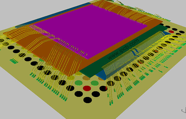
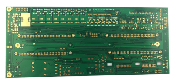
Circuito ad alta frequenza
6) Copper plating: In PCB (high frequency circuit board) design, the interference between signals can be reduced by adding grounded copper foil.
7) Terra coperta: Nella progettazione PCB, quando il cablaggio del circuito stampato ad alta frequenza, coprendo importanti linee di segnale, l'abilità anti-interferenza del segnale può essere significativamente migliorata. Naturalmente, la sorgente di interferenza può anche essere incapsulata per evitare interferenze con altri segnali.
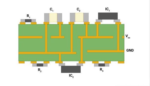
8) Power line: In Progettazione PCB, when the high-frequency circuit board is routed, la rotta del segnale non può generare loop, and must be laid out in accordance with the daisy chain.
9) Condensatore di disaccoppiamento: Nella progettazione PCB, quando il circuito stampato ad alta frequenza è instradato, il condensatore di disaccoppiamento è collegato all'estremità di potenza del circuito integrato.
10) High-frequency choke: In the PCB circuit board design, durante il cablaggio del circuito ad alta frequenza, the digital ground wire and the analog ground wire need to be connected with a high-frequency choke device, di solito un ferro ad alta frequenza attraverso il foro centrale Perle di ferrite.
iPcb is a high-tech manufacturing enterprise focusing on the development and production of high-precision PCBs. iPCB è felice di essere il tuo partner commerciale. Our business goal is to become the most professional prototyping Produttore di PCBnel mondo. Mainly focus on microwave high frequency PCB, pressione mista ad alta frequenza, Test IC multistrato ultra-alto, from 1+ to 6+ HDI, Anylayer HDI, IC Substrate, Scheda di prova IC, rigid flexible PCB, PCB FR4 multistrato ordinario, etc. I prodotti sono ampiamente utilizzati nell'industria 4.0, communications, controllo industriale, digital, power, computers, automobili, medical, aerospaziale, instrumentation, Internet of Things e altri campi.