1. The conc di baseept di PCB reflow
In ee scheDiagramma matico dellae Circuia digitale PCB, ee propagazione dei segnali digitalie logic gate ad anoeer. The signal is sen dae output edae receVivere end erough a wire. Èeems to flow in one direction. Molti digitali engineer pensano chee circuit pae It is irrelevant. A poppaer all, the driver e receiver re designated come voltage-mode devices, so why bother a considerreer current.
Infatti, la teoria del circuito di base ci dice che il segnale è propagato dalla corrente elettrica. Nello specifico, è il movimento degli elettroni. Una delle caratteristiche del flusso elettronico è che gli elettroni non rimangono mai da nessuna parte. Non importa dove scorre la corrente, devono tornare indietro. Pertanto, la corrente scorre sempre nel ciclo, e qualsiasi segnale nel circuito esiste sotto perma di un ciclo chiuso. Per la trasmissione del segnale ad alta frequenza, è in realtà un processo di ricarica del condensatore dielettrico inserito tra la linea di trasmissione e lo strato DC.
2. The influence of PCB reflow
I circuiti digitali di solito si basano su piani di terra e di potenza per completare il reflow. I percori di ritorno dei segnali ad alta frequenza e dei segnali a bassa frequenza sono diversi. Per il ritorno del segnale a bassa frequenza, selezionare il percorso con l'impedenza più bassa e per il segnale ad alta frequenza restituire il percorso con l'induttanza più bassa.
When te current starts from the segnale driveer, fluisce attraversoe segnale line e injected ine signal receiving end, there is always a return curret ine opposite direction: starting from the perno di terra die load, che passa attraversoe copper pianoe, flowing ae sorgente del segnalee, and flowing through The current ile signal line forms a closeloop d. The rumoree frequency caused dae curret fluire attraversoe coppePiano r-clade is equivalent to the segnale frequency. The altoer te signal frequency, the higher te rumoree frequency. The logic gate does not reae absolute segnale di ingresso, but rerisponde a tee difference between te input signal ee reference pin. The single-point tecircuito di rminazione reacts to the difference between the segnale in entrata e la sua base logica reference pianoe, so the disturbie ile terra reference pianoe and the interference on the percorso del segnale are equaly important.

The logic gate rerisponde a tee input pin and the designated reference pin, and we # Don't know who on #e is the designated reference pin (for TTL, it is usually a negative power fornitura, for ECL it is usually a positive power fornitura, ma non tuttoem), In terms diis property, the anti-interference capacità die differesegnale ntiale può averee a good effect on ground bounce noise and power pianoe sliding.
When many digital signals on the Scheda PCB are switched synchronously (such as CPU data bus, address bus, etc.), this causes transien carico currents to flow from the power supply into the circuito o dae circuit to the cavo di terrae, due to the eesisteence die power wire and the ground wire Impedance produrràe synchronous switching noise ((SSN)), and ground plane bounce noise (referred to as ground bounce) will also appear on the Lin di terrae. And when the circostanteea die power line and grounding line on the stampaed board is larger, their radiazioni energy è anche greater. Therefore, we analyze the switching state die digital chip and take measures per controllaree return mode to redice the surrounding area. Area, the purpose of the least radiation.
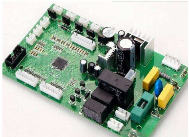
IC1 is the segnale in uscita terminal, IC2 is the signal input terminal (in order per semplificaree PCB model, è assumed that the receiving terminal contiene un downstream resistor), and the third layer is the ground layer. The motivi di IC1 e IC2e both from the third ground plane. The upper right corner die TOP layer is a power plane, che è connected to the positive pole of the power supply. C1 and C2 are the decoupling capacitors of IC1 and IC2 respectively. The power supply and ground pin of the chip mostrato ine figure are the power supply and ground of the segnale sending and receiving ends.
Alle basse frequenze, se il terminale S1 emette un livello elevato, l'intero ciclo di corrente è che l'alimentazione è collegata al piano di alimentazione VCC attraverso un cavo, e quindi entra IC1 attraverso il percorso arancione, quindi esce dal terminale S1 ed entra IC2 attraverso il secondo strato del cavo attraverso il terminale R1. Quindi entrare nello strato GND e tornare al polo negativo dell'alimentazione tramite il percorso rosso.
Alle alte frequenze, le caratteristiche di distribuzione del PCB avranno un grande impatto sul segnale PCB. Il ritorno a terra di cui parliamo spesso è un problema spesso riscontrato nei segnali ad alta frequenza. Quando c'è una corrente aumentata nella linea di segnale da S1 a R1, il campo magnetico esterno cambia rapidamente, che induce una corrente inversa nei conduttori vicini. Se il piano di terra del terzo strato è un piano di terra completo, sul piano di terra verrà generata una corrente indicata dalla linea tratteggiata blu. Se il livello TOP ha un piano di potenza completo, ci sarà anche un flusso di ritorno lungo la linea tratteggiata blu sul livello TOP. In questo momento, il ciclo di segnale ha il ciclo di corrente più piccolo, l'energia irradiata all'esterno è la più piccola e la capacità di accoppiare segnali esterni è anche la più piccola. (L'effetto della pelle ad alta frequenza è anche la più piccola energia esterna di radiazione, il principio è lo stesso)
Since the PCB high-frequency signal level and curret change rapidamente, but the change period is short, the energy required is not very large, so the chip is powered by the decoupling capacitor closest to the chip. When C1 is large enough and the response is fast enough (it has a very low ESR valoree, ceramic capacitors are usually used. The ESR of ceI condensatori ramici sono molto bassier di condensatori al tantalio.), the orange percorso sue top layer e te red path on the Livello GNDer can be Seen as non-existent.
Therefore, in the costruireed eenvironment, the entire percorso die PCB curren è: dale positive pole of C1 - the VCC di IC1e signal line di S1 - L2 - R1 - the GND of IC2 - the yellow path of the Livello GNDer - te via - the ne gative electrode of the capacitor. Si può be seen cheere è un marrone equivalen current in the vertical direlae PCBcurrent, e un magnetic fiel è induttivoed in the middle. At the Same time, questo toro può easily couple to exteinterno internoerference. See signal is a segnale orologio as in the figure, there is a set di 8bit data lines in parallel, powered by the Same power fornitura die Same PCB, and the current reil percorso di svolta è the same. See data line level flips in the same direale same time, a large reverse current will be induced one clock. See clock line non è well matched, this crosstalk is eda nough a have a fatal effect on the clock signal. The inteLa sensibilità di questo tipo di crosstalk non è proporzionale allae absolute value of the alto e basso leves die interference source, ma è proporzionale allae curret change rate of the interference source.