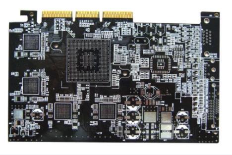
PCB board layout rules
1) Under normal circumstances, all components should be arranged on the same side of the circuit board. Only when the top components are too dense, can some devices with limited height and low heat generation, such as chip resistors, chip capacitors, Chip IC, etc. are placed on the bottom layer.
2) On the premise of ensuring electrical performance, components should be placed on the grid and arranged parallel or perpendicular to each other to be neat and beautiful. In general, components are not allowed to overlap; the arrangement of components should be compact, and components should be placed on the entire layout. The distribution is uniform and the density is consistent.
3) The small spacing between adjacent pad patterns of different components on the circuit board should be more than 1MM.
4) The distance from the edge of the circuit board is generally not less than 2MM, the best shape of the circuit board is a rectangle, and the aspect ratio is 3:2 or 4:3. When the size of the circuit board is larger than 200MM by 150MM, the mechanical strength that the circuit board can bear should be considered.
PCB board design setup skills
The PCB board design requires different point settings at different stages. In the layout stage, large grid points can be used for device layout. For large devices such as ICs and non-positioning connectors, 50-100 mil grid points can be used for layout, while for passive small devices such as resistors, capacitors and inductors, 25 mil grid points can be used for layout. The large grid points facilitate the alignment of the device and the aesthetics of the layout.
PCB board design layout skills
In the layout design of the PCB board, the unit of the circuit board should be analyzed, and the layout design should be carried out according to the function. When laying out all the components of the circuit, the following principles should be followed:
1) Arrange the position of each functional circuit unit according to the circuit process, so that the layout is convenient for signal circulation, and the signal keeps the same direction as possible.
2) Take the components of each functional unit as the center, and arrange the layout around him. Components should be evenly, integrally and compactly arranged on the PCB board, and the leads and connections between components should be minimized and shortened.
3) For circuits operating at high frequencies, the distribution parameters between components should be considered. In general, the components should be arranged in parallel as far as possible, which is not only beautiful, but also easy to install and mass-produce.
The following points should be paid attention to when designing the specific wiring of the PCB board:
1) Keep the trace length as short as possible to minimize lead inductance. In low frequency circuits, multipoint grounding is avoided because all circuit ground currents flow through a common ground impedance or ground plane.
2) The common ground wire should be arranged at the edge of the printed circuit board as much as possible. As much copper foil as possible should be reserved on the circuit board as the ground wire, which can enhance the shielding ability.
3) The double-layer board can use the ground plane. The purpose of the ground plane is to provide a low-impedance ground wire.
4) In the multi-layer printed circuit board, the ground layer can be set, and the ground layer is designed into a mesh. The grid spacing of the ground wire should not be too large, because one of the main functions of the ground wire is to provide a signal return path. If the grid spacing is too large, a larger signal loop area will be formed. Large loop areas can cause radiation and sensitivity problems. In addition, the signal return actually takes a path with a small loop area, and other ground wires do not work.
5) The ground plane can make the radiation loop small on the
PCB board.