

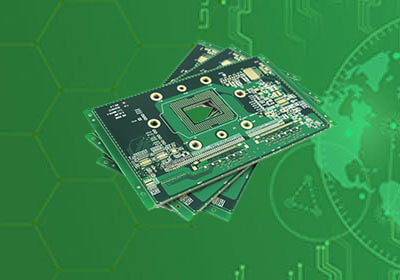
PCB board is the mother of electronic products. It also known as a Printed circuit board (PCB) or Printed wire board(PWB), is a provider of electrical connections for electronic components.it is an electronic component that uses electronic printing to etch on the surface of the insulated and nonbinding copper-clad laminate, leaving a network of small circuits so that various electronic components can form a predetermined circuit connection and achieve the relay transmission function between electronic components. Most electronic equipment and products need to be equipped with a PWB Board.
Printed circuit boards are often referred to as PWB, and also have many people called PCB substrate. Since the printed circuit board is not a general terminal product, the definition of the name is slightly confusing. For example, the motherboard for personal computers is called the mainboard, and cannot be directly called the circuit board. Although there are circuit boards in the motherboard, They are not the same, so when evaluating the industry, the two are related but cannot be said to be the same. Another example: because there are integrated circuit components mounted on the circuit board, the news media call it an IC board, but in fact, it is not equivalent to a printed circuit board. We usually say that the printed circuit board refers to the bare board-that the circuit board without upper components.
According to the number of electronic board layers, it can be divided into single-sided, double-layer, four-layer, six-layer, and other multilayer circuit boards. And continue to develop in the direction of high precision, high density, and high reliability. Continuously shrinking volume, reducing costs, and improving performance have enabled printed circuit boards to maintain strong vitality in the development of future electronic products. The future development trend of PWB manufacturing technology is to develop in the direction of high density, high precision, fine aperture, fine wire, small pitch, high reliability, multilayer, high-speed transmission, lightweight, and thinness in performance.

PCB
According to the distribution of printed circuit boards
Single-sided PCB substrate
The single layer is on an insulating substrate with a thickness of 0.2-5mm, only one surface is covered with copper foil, and a printed circuit is formed on the substrate by printing and etching. The single panel is simple to manufacture and easy to assemble. It is suitable for the requirements of a circuit, such as radios, televisions, etc. It is not suitable for occasions requiring high assembly density or complex circuits.
Double-sided pcb substrate
The double-sided boards are printed circuits on both sides of an insulating substrate with a thickness of 0.2-5mm. It is suitable for electronic products with general requirements, such as electronic computers, electronic instruments, and meters. Since the wiring density of the double-sided printed circuit is higher than that of the single-sided printed circuit, the volume of the device can be reduced.
Multilayer PCB plate
Printed panels with more than 3 layers of printed circuits printed on an insulating substrate are called multilayer panels. It is a combination of several thin single or double panels, and its thickness is generally 1.2-2.5mm. In order to lead out the circuit sandwiched between the insulating substrate, the holes for mounting components on the multilayer board need to be metalized, that is, a metal layer is applied to the inner surface of the small holes to connect them with the printed circuit sandwiched between the insulating substrates.
Classified by the nature of the substrate
Rigid PCB substrate
The rigid PWB has a certain mechanical strength, and the parts assembled with it have a flat state. Rigid printed panels are used in general electronic products.
Flex PCB substrate
The flexible PWB is made of soft layered plastic or other soft insulating materials as the base material. The parts made of it can be bent and stretched and can be bent according to the installation requirements during use. Flexible printed boards are generally used on special occasions. For example, the display screen of some digital multimeters can be rotated, and flexible printed boards are often used inside; the display screens, buttons of mobile phones, etc.
Rigid-flex PCB substrate
The birth and development of FPC and PWB gave birth to the new product of flex and rigid board. Therefore, the rigid-flex board is the flexible circuit board and the rigid circuit board. After pressing and other processes, they are combined according to the relevant process requirements to form an electronic board with FPC characteristics and PWB characteristics.

Classified by the scope of application
PWB can be divided into low-frequency PCB and high-frequency PCB. High frequency of electronic equipment is the development trend, especially in today's wireless network and satellite communication, information products are moving towards high speed and high frequency, and communication products are moving towards the standardization of voice, video, and data of wireless transmission with large capacity and high speed. Therefore, the new generation of products needs a high-frequency printed circuit board, and the foil substrate can be made up of materials with small dielectric loss and dielectric constant, such as polyurethane, polyethylene, polystyrene, polytetrafluoroethylene glass cloth.
Classified by the special printed boards
At present, there are some specially printed boards, such as metal core printed board, surface mounted printed circuit board, and carbon film printed board.
Metal core PCB plate
The metal core circuit board is to replace the epoxy glass cloth board with a metal plate of the same thickness. After special treatment, the conductor circuits on both sides of the metal board are connected with each other and highly insulated from the metal part. The advantage of metal core PCB is good heat dissipation and dimensional stability. This is because magnetic materials such as aluminum and iron have a shielding effect and can prevent mutual interference.
Surface mount PCB
Surface mount printed circuit board (SMB) is a kind of PWB developed to meet the needs of light, thin, short and small electronic products, and with the installation process of surface mount devices with pin density and low cost. The printed circuit board has the characteristics of a small aperture, small line width and spacing, high precision, and high substrate requirements.
Carbon film printed substrate
Carbon film printed board is a kind of printed board that is printed with a layer of carbon film after the conductor pattern is made on the copper foil to form contact or jumper wire (the resistance value meets the specified requirements). It is characterized by a simple production process, low cost, short cycle, good wear resistance, and electrical conductivity.It can realize the high density of single panels and miniaturization and light weight of products. It is suitable for TV, telephone, video recorder, and electronic organ.
How to design PCB substrate?
When designing a circuit board, many complicated steps are often required. Whether it is the basics of micro-processing copper and solder or trying to ensure that the PWB is finally printed, or encountering more specific design problems, such as through-hole technology or design signals with through-holes, pads, and any number of layouts For integrity issues, you need to ensure that you have the correct design software. So now iPCB tells you how to design a PCB panel.
1. Create a schematic diagram of the PCB substrate
Whether you are generating a design from a template or creating a PCB panel from scratch, it is best to start with a PWB schematic. The schematic is similar to the blueprint of the new device, and it is important to understand what is shown in the schematic. Compared with designing directly on the PCB panel, not only is the circuit interconnection easier to define and edit, but it is also much easier to convert the PWB schematic diagram into the PWB board layout. For components, PCB circuit board design software has an extensive part library database.
2. Create a blank PCB plate layout
After creating the PWB schematic, you need to use the schematic capture tool in the PCB design software to start creating the PCB layout. Before that, you need to create a blank PCB document. To create a PCB panel, a PCB Doc file needs to be generated. This can be done easily from the main menu of the design software
If the PCB shape, size, and layer stack of the PWB panel have been determined, you can set it up immediately. If you don't want to perform these tasks now, don't worry, you can change the shape of the PCB plate later. By compiling SchDoc, the schematic information can be used in PCB. The compilation process includes verifying the design and generating several project documents so that you can check and correct the design before transferring to PCB. It is strongly recommended that you check and update the item options used to create the PCB information at this time.
When designing a PWB panel, it sometimes seems that it will be a long and arduous journey to reach the final design. Whether it is the basics of micro-processing copper and solder trying to ensure that the PWB is finally printed, or encountering more specific design problems, such as through-hole technology or design signals with through-holes, pads, and any number of layouts For integrity issues, you need to ensure that you have the correct PWB design software.
3. Capture the schematic diagram of the PCB prototype board and link it to the PCB
All the tools in the PCB prototype substrate design software can be used in a unified design environment. In this design environment, the schematic, PCB, and BOM are related to each other and can be accessed at the same time. Other programs will force you to manually compile the schematic data.
4. Design the PCB stack up
When you transfer the schematic information to PCB Doc, in addition to the specified PCB plate outline, the package of the component will also be displayed. Before placing components, you should use the "Layer Stack Manager" as shown below to define the PCB layout (ie shape, layer stack).
If you are not familiar with PWB plate design, although any number of layers can be defined in the PWB panel design software, most modern designs will start with a 4-layer board on FR4. You can also take advantage of the material stacking library; this way, you can choose from a variety of different laminates and unique panels.
If you want to design a high-speed/high-frequency circuit board, you can use the built-in impedance analyzer to ensure impedance control in the PCB prototype board. The impedance curve tool uses Simberian's integrated electromagnetic field solver to customize the geometry of the trace to achieve the target impedance value.
For more detailed PWB stack-up reference instructions, click Download - ![]()
5. Define design rules and DFM requirements
There are many categories of PWB design rules, and you may not need to use all of these available rules for every design. You can select/deselect individual rules by right-clicking the problematic rule in the list in the PWB rule and constraint editor below.
The rules you do use, especially those used for manufacturing, should comply with the specifications and tolerances of the PCB manufacturer’s equipment. Advanced designs such as impedance control designs and many high-speed/high-frequency designs may need to follow very specific design rules to ensure that your product works properly. Always check your component datasheet to understand these design rules.
6. Place the components on the PWB prototype substrate
The current mainstream PWB board design software provides great flexibility and allows you to quickly place components on the circuit board. You can arrange the components automatically, or you can place them manually. You can also use these options together to take advantage of the speed of automatic placement and ensure that the PWB is laid out according to good component placement guidelines.
7. PWB board insertion hole
Before the PWB layout, it is best to place drill holes (mounting and vias). If your design is complex, you may need to modify at least some via locations during the routing process. This can be done easily through the "Properties" dialog box.
Your preference here should follow the manufacturing design (DFM) specifications of the circuit board manufacturer. If you have defined the DFM requirements of the PWB as design rules (see step 5), the PWB design software will automatically check these rules when you place vias, drill holes, pads, and traces in the layout.
8. PWB plate layout tracking
After placing the components and any other mechanical components, you can prepare the layout. Make sure to use good wiring guidelines and PWB design software tools to simplify the process, such as highlighting the net and color coding through wiring.
9. Add the label and identifier of the PWB
After verifying the PWB layout, you can add labels, identifiers, marks, logos, or any other images on the pcb plate. It is a good idea to use reference identifiers for components, as this will help PWB assembly. In addition, include polarity indicators, pin 1 indicators, and any other labels that help identify components and their orientation. For logos and images, it is best to consult your PWB board manufacturer to ensure that the fonts you use are readable.
10. Generate the Gerber file for the design of the PCB Layout.
Before the PCB manufacturer can deliver the results, it is always best to verify the PCB layout by running a design rule check (DRC).
After the PWB board passes the final DRC, you need to generate design files for the PCB board manufacturer. The design file should include all the information and data needed to build it, and include any notes or special requirements to ensure that your manufacturer is clear about your requirements. For most PCB manufacturers, you will be able to use Gerber files, but some pcb plate manufacturers prefer other CAD file formats. Now, do you know what is PCB?


