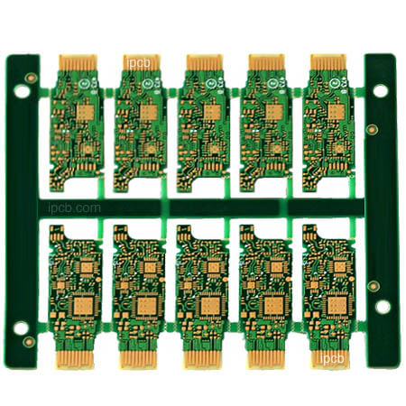
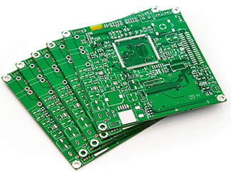
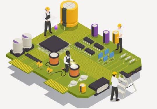
Il PCB, noto anche come circuiti stampati, può realizzare la connessione del circuito e la realizzazione della funzione tra i componenti elettronici ed è anche una parte importante della progettazione del circuito di alimentazione. Oggi, questo articolo introdurrà le regole di base del layout e del cablaggio PCB.

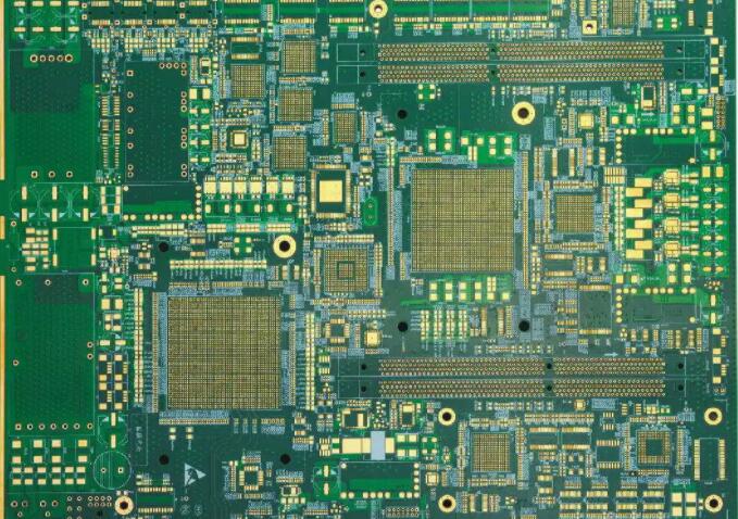
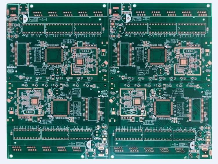
1. Regole di base del layout componente1. Layout secondo il modulo del circuito, i circuiti correlati che realizzano la stessa funzione sono chiamati modulo, i componenti nel modulo del circuito dovrebbero adottare il principio della concentrazione vicina e il circuito digitale e il circuito analogico dovrebbero essere separati; 2. non montare componenti e dispositivi entro 1.27mm intorno a fori non di montaggio come fori di posizionamento e fori standard, e non montare componenti entro 3.5mm (per M2.5) e 4mm (per M3) intorno a fori di montaggio come viti; 3. evitare di posizionare vias sotto componenti come resistenze montate orizzontalmente, induttori (plug-in) e condensatori elettrolitici per evitare cortocircuiti tra vias e il guscio del componente dopo la saldatura ad onda; 4. la distanza tra l'esterno del componente e il bordo del bordo è 5mm; 5. la distanza tra l'esterno del pad del componente montato e l'esterno del componente adiacente è maggiore di 2mm; 6. i componenti del guscio metallico e le parti metalliche (scatole di schermatura, ecc.) non possono toccare altri componenti e non possono essere vicini alle linee e ai pad stampati e la distanza dovrebbe essere maggiore di 2mm. La dimensione dei fori di posizionamento, dei fori di installazione del fermo, dei fori ellittici e degli altri fori quadrati nella piastra è maggiore di 3mm dal bordo della piastra; 7. l'elemento riscaldante non può essere vicino al filo e all'elemento termico; l'elemento ad alto riscaldamento dovrebbe essere distribuito uniformemente; 8. La presa di corrente dovrebbe essere disposta intorno alla scheda stampata il più possibile e i terminali della barra del bus collegati alla presa di corrente dovrebbero essere disposti sullo stesso lato. Particolare attenzione deve essere prestata a non disporre prese di corrente e altri connettori saldati tra i connettori, al fine di facilitare la saldatura di queste prese e connettori, nonché la progettazione e la legatura dei cavi di alimentazione. Per facilitare l'inserimento e la rimozione delle spine di alimentazione deve essere considerata la distanza di disposizione delle prese di alimentazione e dei connettori di saldatura; 9. disposizione di altri componenti: tutti i componenti IC sono allineati su un lato, i componenti polari sono contrassegnati chiaramente e la marcatura di polarità sulla stessa scheda stampata non dovrebbe essere più di due direzioni. Quando appaiono due direzioni, le due direzioni sono perpendicolari l'una all'altra.; 10. Il cablaggio sulla scheda dovrebbe essere correttamente denso. Quando la differenza di densità è troppo grande, dovrebbe essere riempita con foglio di rame mesh e la maglia dovrebbe essere maggiore di 8mil (o 0,2mm); 11. Non ci dovrebbero essere fori passanti sui cuscinetti patch, in modo da evitare la perdita di pasta di saldatura e causare la saldatura dei componenti. Le linee di segnale importanti non sono permesse di passare tra i pin della presa; 12. la patch è allineata unilateralmente, la direzione del carattere è la stessa e la direzione dell'imballaggio è la stessa; 13. Per i dispositivi con polarità, la direzione della marcatura di polarità sulla stessa scheda dovrebbe essere il più coerente possibile.2. Regole di cablaggio componenteNella zona in cui l'area di cablaggio si trova â¤1mm dal bordo del PCB e entro 1mm intorno al foro di montaggio, il cablaggio è vietato; 2. la linea elettrica dovrebbe essere il più ampia possibile e non dovrebbe essere inferiore a 18mil; la larghezza della linea di segnale non deve essere inferiore a 12mil; CPU Le linee in entrata e in uscita non devono essere inferiori a 10mil (o 8mil); la distanza tra le linee non dovrebbe essere inferiore a 10mil; 3, il foro via normale non dovrebbe essere inferiore a 30mil; 4, il doppio in linea: pad 60mil, apertura 40mil; 55mil (0805 montaggio superficiale); 62mil pad, 42mil apertura quando collegato direttamente; condensatore elettrodeless: 51 * 55mil (0805 supporto superficiale); 50mil pad, 28mil apertura quando collegato direttamente; 5. Si noti che il cavo di alimentazione e il cavo di massa dovrebbero essere il più possibile radiali e la linea di segnale non può avere loopback.
2.1 I seguenti sistemi dovrebbero prestare particolare attenzione alle interferenze elettromagnetiche:(1) La frequenza di clock del microcontrollore è particolarmente elevata e il ciclo bus è particolarmente rapido. (2) Il sistema contiene circuiti di azionamento ad alta potenza e ad alta corrente, quali relè generatore di scintille, interruttori ad alta corrente, ecc. (3) Un sistema con un circuito di segnale analogico debole e un circuito di conversione A/D ad alta precisione.2.2 Per aumentare la capacità di interferenza anti-elettromagnetica del sistema, prendere le seguenti misure:(1) Selezionare un microcontrollore con bassa frequenza: La selezione di un microcontrollore con bassa frequenza esterna di clock può efficacemente ridurre il rumore e migliorare la capacità anti-interferenza del sistema. Onde quadrate e onde sinusoidali della stessa frequenza, i componenti ad alta frequenza nell'onda quadrata sono molto più dell'onda sinusoidale. Sebbene l'ampiezza della componente ad alta frequenza dell'onda quadrata sia inferiore a quella dell'onda fondamentale, maggiore è la frequenza, più facile è emettere e diventare una fonte di rumore. L'influente rumore ad alta frequenza generato dal microcontrollore è circa 3 volte la frequenza dell'orologio.
(2) Ridurre la distorsione nella trasmissione del segnale Il microcontrollore pricipalmente è fabbricato con tecnologia CMOS ad alta velocità. La corrente di ingresso statica del terminale di ingresso del segnale è di circa 1mA, la capacità di ingresso è di circa 10PF, l'impedenza di ingresso è abbastanza alta e il terminale di uscita del circuito CMOS ad alta velocità ha una notevole capacità di carico, cioè un valore di uscita considerevole. Il problema di riflessione è molto grave quando la lunga linea è condotta all'estremità di ingresso con un'impedenza di ingresso relativamente elevata, che causerà distorsioni del segnale e aumenterà il rumore del sistema. Quando Tpd>Tr, diventa un problema della linea di trasmissione e problemi come la riflessione del segnale e la corrispondenza dell'impedenza devono essere considerati. Il tempo di ritardo del segnale sul circuito stampato è correlato all'impedenza caratteristica del cavo, cioè alla costante dielettrica del materiale del circuito stampato. Si può approssimativamente considerare che la velocità di trasmissione del segnale sui cavi stampati è di circa 1/3 a 1/2 della velocità della luce. Il Tr (tempo di ritardo standard) degli elementi telefonici logici comunemente usati in sistemi composti da microcontrollori è compreso tra 3 e 18 ns. Sul circuito stampato, il segnale passa attraverso una resistenza 7W e un cavo lungo 25cm e il tempo di ritardo on-line è approssimativamente compreso tra 4 e 20ns. Vale a dire, più brevi sono i cavi del segnale sul circuito stampato, meglio è e la lunghezza non dovrebbe superare i 25cm. E il numero di vias dovrebbe essere il più piccolo possibile, non più di 2. Quando il tempo di aumento del segnale è più veloce del tempo di ritardo del segnale, viene elaborato secondo elettronica veloce. In questo momento, si dovrebbe considerare la corrispondenza dell'impedenza della linea di trasmissione. Per la trasmissione del segnale tra i blocchi integrati su un circuito stampato, è necessario evitare la situazione di Td>Trd. Più grande è il circuito stampato, meno la velocità del sistema può essere troppo veloce. Una regola generale per la progettazione del circuito stampato è riassunta dalle seguenti conclusioni: Il tempo di ritardo della trasmissione del segnale sul circuito stampato non deve essere superiore al tempo di ritardo nominale del dispositivo utilizzato.
(3) Ridurre l'interferenza tra le linee del segnale:Un segnale di passo con un tempo di salita di Tr al punto A è trasmesso al terminale B attraverso il cavo AB. Il tempo di ritardo del segnale sulla linea AB è Td. Al punto D, a causa della trasmissione in avanti del segnale al punto A, la riflessione del segnale dopo aver raggiunto il punto B e il ritardo della linea AB, un segnale di impulso pagina con una larghezza di Tr sarà indotto dopo il tempo di Td. Al punto C, a causa della trasmissione e della riflessione del segnale su AB, sarà indotto un segnale di impulso positivo con una larghezza del doppio del tempo di ritardo del segnale sulla linea AB, cioè 2Td. Questa è l'interferenza incrociata tra i segnali. La forza del segnale interferente è correlata al di/at del segnale al punto C ed è correlata alla distanza tra le linee. Quando le due linee di segnale non sono molto lunghe, ciò che in realtà si vede su AB è la sovrapposizione di due impulsi. I microcontrollori fabbricati dal processo CMOS hanno un'elevata impedenza di ingresso, alto rumore e alta tolleranza al rumore. Il circuito digitale è sovrapposto al rumore di 100 ~ 200mv e non influisce sul suo lavoro. Se la linea AB nella figura è un segnale analogico, questo tipo di interferenza diventa intollerabile. Ad esempio, se il circuito stampato è una scheda a quattro strati, uno dei quali è un terreno di grande area, o una scheda bifacciale, quando il lato opposto della linea del segnale è un terreno di grande area, l'interferenza incrociata tra tali segnali diventerà più piccola. La ragione è che la grande area di terra riduce l'impedenza caratteristica della linea di segnale e la riflessione del segnale al terminale D è notevolmente ridotta. L'impedenza caratteristica è inversamente proporzionale al quadrato della costante dielettrica del mezzo tra la linea del segnale e il terreno ed è proporzionale al logaritmo naturale dello spessore del mezzo. Se la linea AB è un segnale analogico, per evitare l'interferenza della linea di segnale del circuito digitale CD ad AB, ci dovrebbe essere una grande area di terra sotto la linea AB e la distanza dalla linea AB alla linea CD dovrebbe essere maggiore di 2 ~ 3 volte la distanza tra la linea AB e la terra. Può essere utilizzata una schermatura parziale e i fili di terra sono disposti sui lati sinistro e destro del cavo sul lato con la giunzione del cavo.
(4) Ridurre il rumore dell'alimentazione elettrica Mentre fornisce energia al sistema, l'alimentazione aggiunge anche il suo rumore all'alimentazione elettrica fornita. La linea di reset, la linea di interruzione e altre linee di controllo del microcontrollore nel circuito sono facilmente disturbate dal rumore esterno. Forti disturbi sulla rete entrano nel circuito attraverso l'alimentazione elettrica, e anche nei sistemi alimentati a batteria, la batteria stessa ha rumore ad alta frequenza. I segnali analogici nei circuiti analogici sono più resistenti alle interferenze provenienti da fonti di alimentazione.
(5) Prestare attenzione alle caratteristiche ad alta frequenza dei circuiti stampati e dei componenti. In caso di alta frequenza, i cavi, i vias, le resistenze, i condensatori e l'induttanza e la capacità distribuiti dei connettori sul circuito stampato non possono essere ignorati. L'induttanza distribuita del condensatore non può essere ignorata e la capacità distribuita dell'induttore non può essere ignorata. La resistenza rifletterà il segnale ad alta frequenza e la capacità distribuita del cavo funzionerà. Quando la lunghezza è maggiore di 1/20 della lunghezza d'onda corrispondente della frequenza del rumore, si verificherà un effetto antenna e il rumore sarà emesso attraverso il cavo. I vias del circuito stampato causano una capacità di circa 0.6pf. Il materiale di imballaggio di un circuito integrato introduce la capacità di 2 ~ 6pf. Un connettore su un circuito stampato ha un'induttanza distribuita di 520nH. Un supporto di circuito integrato a 24 pin dritto a doppia fila, che introduce un'induttanza distribuita di 4~18nH. Questi piccoli parametri di distribuzione sono trascurabili per questa linea di sistemi microcontrollori a frequenze inferiori; occorre prestare particolare attenzione ai sistemi ad alta velocità.
(6) La disposizione dei componenti dovrebbe essere ragionevolmente suddivisa. La posizione dei componenti disposti sul circuito stampato deve essere pienamente considerata contro le interferenze elettromagnetiche. Uno dei principi è che i cavi tra i componenti devono essere il più brevi possibile. Nel layout, la parte del segnale analogico, la parte del circuito digitale ad alta velocità e la parte della sorgente di rumore (come relè, interruttori ad alta corrente, ecc.) dovrebbero essere ragionevolmente separati, in modo che i segnali tra di loro siano accoppiati l'uno all'altro. Gestire il cavo di massa sul circuito stampato, il cavo di alimentazione e il cavo di massa sono importanti. Per superare le interferenze elettromagnetiche, il mezzo principale è la messa a terra. Per il pannello bifacciale, il layout del filo di terra è molto particolare. Adottando il metodo di messa a terra a punto singolo, l'alimentazione elettrica e la terra sono collegati al circuito stampato da entrambe le estremità dell'alimentazione elettrica, con un contatto per l'alimentazione elettrica e un contatto per la terra. Sul circuito stampato, ci devono essere più fili di terra di ritorno e questi saranno raccolti al contatto dell'alimentatore di ritorno, che è la cosiddetta messa a terra a punto singolo. La cosiddetta separazione di terra analogica, terra digitale e terra del dispositivo ad alta potenza significa che il cablaggio è separato e tutti sono riuniti in questo punto di messa a terra. Quando si collega a segnali diversi dal circuito stampato, vengono solitamente utilizzati cavi schermati. Per segnali digitali e ad alta frequenza, il cavo schermato è messo a terra ad entrambe le estremità. I cavi schermati per segnali analogici a bassa frequenza devono essere messi a terra ad un'estremità. I circuiti che sono molto sensibili al rumore e alle interferenze o circuiti che sono particolarmente rumore della scheda PCB ad alta frequenza dovrebbero essere schermati con una copertura metallica.