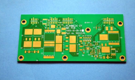
一般的なPCB表面処理プロセス
はじめに PCB多層回路基板 表面処理技術は、PCB構成要素上の表面層の層の人工形成と、機械的とは異なる電気接続点を指す, 基板の物理的性質と化学的性質. その目的は、PCBの良好なはんだ付け性または電気的性質を確保することである. なぜなら、銅は空気中の酸化物の形で存在するからです, PCBのはんだ付け性と電気的性質に重大に影響するPCB, 表面処理を行う必要がある PCB multilayer 回路基板.
The common surface treatment methods are as follows:
1, hot air leveling
The process of coating molten tin-lead solder on the surface of the PCB and flattening (flattening) with heated compressed air to form a coating layer that is resistant to copper oxidation and provides good solderability. 熱気中, はんだ及び銅は接合部に銅−錫−金属化合物を形成する, and the thickness is about 1 to 2 mils;
2, chemically immersed nickel gold
A thick layer of nickel-gold alloy with good electrical properties is wrapped on the copper surface and can protect the PCB for a long time. OSPと違って, 防錆バリア層としてのみ使用される, PCBの長期使用において有用であり、良好な電気的性能を達成することができる. 加えて, it also has tolerance to the environment that other surface treatment processes do not have;
3, chemical immersion silver
Between OSP and electroless nickel/ゴールドイマージョン, プロセスはより簡単で、より速い. 熱にさらされると, 湿度と汚染, それはまだ良い電気性能を提供し、良好なはんだ付け性を維持することができます, しかし、それは光沢を失う. 銀層の下にはニッケルがないからです, 浸漬銀は無電解ニッケルの良い物理的強度を持っていない/immersion gold;

4, organic anti-oxidation (OSP)
On the clean bare copper surface, 有機フィルムのレイヤーは、化学的に育てられる. フィルムのこの層は、酸化防止を有する, 耐熱衝撃性, and moisture resistance to protect the copper surface from rusting (oxidation or sulfidation, etc.) in a normal environment; at the same time, it must be easily assisted in the subsequent welding high temperature The flux is quickly removed to facilitate welding;
5, electroplating nickel gold
The conductor on the PCB surface is electroplated with a layer of nickel and then electroplated with a layer of gold. ニッケルめっきの主な目的は金と銅の拡散を防ぐことである. There are two types of electroplated nickel gold: soft gold plating (pure gold, gold indicates that it does not look bright) and hard gold plating (the surface is smooth and hard, 耐摩耗性, コバルトその他の元素を含む, and the surface looks brighter). Soft gold is mainly used for gold wire during chip packaging; hard gold is mainly used for electrical interconnection in non-soldering places (such as gold fingers).
6, PCB多層回路基板 mixed surface treatment technology
Choose two or more surface treatment methods for surface treatment. The common forms are: Immersion Nickel Gold + Anti-oxidation, Electroplating Nickel Gold + Immersion Nickel Gold, Electroplating Nickel Gold + Hot Air Leveling, Immersion Nickel Gold + Hot Air Leveling .
全表面処理法, hot air leveling (lead-free/leaded) is the most common and cheapest treatment method, しかし、EUのRoHS規制に注意を払ってください.
RoHSは:EUの法律によって確立された義務的な基準. Its full name is "Restriction of Hazardous Substances" (Restriction of Hazardous Substances). 規格は7月1日に正式に実施されている, 2006年, そして、主に電気および電子製品の材料およびプロセス標準を標準化するために使用される, 人間の健康と環境保護をより促進する. この規格の目的は、鉛を含む6つの物質を除去することである, 水銀, カドミウム, 六価クロム, 電気及び電子製品中のポリ臭化ビフェニル及びポリ臭化ジフェニルエーテル, そして、それは、特に鉛含有量が0を超えないことを規定します.1 %.
IPCBは、高精度のPCBの開発と生産に焦点を当てたハイテク製造企業です. iPCBは、あなたのビジネスパートナーであることを幸せです. 当社のビジネス目標は、最もプロフェッショナルなプロトタイピングになることです PCBメーカー 世界で. 主にマイクロ波高周波PCBに注目, 高周波混合圧力, 超高多層IC試験, from 1+ to 6+ HDI, アンレイヤー, IC基板, ICボード, 剛性フレキシブルPCB, 通常の多層FR 4 PCB, etc. 製品は広く業界で使用されて4.0, コミュニケーション, 産業管理, デジタル, パワー, コンピュータ, 自動車, 医学, 航空宇宙, 計装, ものと他のフィールドのインターネット.