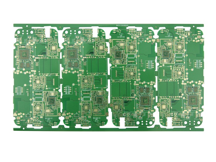
PCB校正の設計, 反ESD PCBの設計 層を通して実現できる, 適切なレイアウトとインストール. デザインプロセスで, 設計変更の大多数は予測を通して部品の追加または減少に制限され得る. 調整することによって PCBボード レイアウトとルーティング, ESDは良好に防止できる. 以下は一般的な予防策です.

*Use multi-layer PCBs as much as possible. 両面PCBと比較して, グランドプレーンとパワープレーン, 密に配置された信号線接地間隔と同様に、コモンモードインピーダンスおよび誘導結合を減少させることができる, それが両面PCBのレベルに達することができるように. /10から1/100. 可能な限り電力層または接地層にそれぞれの信号層を近づけるようにしてください. 上部と底面にコンポーネントを有する高密度PCBs, 短い接続線, 多くのフィールズ, 内側の行を使用することを検討することができます.
*For PCB proofing, 堅く絡み合った電源とグランドグリッドを使用する必要があります. 電力線は接地線に近い, と垂直線と水平線の間に可能な限り多くの接続や充填領域. 一方のグリッドサイズは60 mm以下である. できれば, グリッドサイズは13 mm未満でなければならない.
*Ensure that each circuit is as compact as possible.
* Put all the connectors aside as much as possible.
*If possible, ESDによって直接影響を受ける領域から離れて、カードの中心からの電源コードのリード.
*On all PCB layers below the connector that leads to the outside of the chassis (easy to be directly hit by ESD), 広いシャシーグラウンドまたは多角形の充填地面を置く, そして、約13 mmの距離でビアと一緒にそれらを接続してください. .
*Place mounting holes on the edge of the card, そして、シャシーグラウンドに取り付け穴のまわりでハンダ抵抗なしでトップと底パッドを接続してください.
サンプルアセンブリの間、PCBの上または底のパッドにどんなはんだも適用しないでください. PCBと金属シャシーの間の密接な接触を成し遂げるために、ビルトイン・ワッシャーでネジを使ってください/シールド層又は接地面上の支持体.
*The same "isolation zone" should be set between the chassis ground and circuit ground on each layer; if possible, 分離距離0.64 mm.
* At the top and bottom layers of the card near the mounting holes, シャシーグラウンドと回路グランドを1で接続します.シャーシグランドワイヤーに沿って100 mmごとに27 mmの広いワイヤー. これらの接続点に隣接する, シャシーグラウンドと回路グランドとの間に取り付けるためのパッドまたは取付穴を配置する. これらの接地接続は、回路を開くためにブレードで切断することができる, 磁気ビーズでジャンパー/高周波コンデンサ.
*If the PCB proofing will not be placed in a metal chassis or shielding device, ソルダーレジストは回路基板の上部シャーシ接地配線に適用できない, ESDアークの放電電極として使用できるように.
* To set a ring ground around the circuit in the following way:
(1) In addition to the edge connector and the chassis ground, 全体の周囲に円形のグランドパスが配置される.
(2) Ensure that the ring ground width of all layers is greater than 2.5 mm.
(3) Connect circularly with via holes every 13mm.
(4) Connect the ring ground to the common ground of the 多層回路.
(5) For double panels installed in metal cases or shielding devices, リンググランドは回路の共通のグラウンドに接続されるべきである. 無遮蔽両面回路用, リンググランドはシャシーグラウンドに接続する必要があります. リンググランドにソルダーレジストを塗布してはならない, リンググランドがESD放電バーとして働くことができるように. Place at least one at a certain position on the ring ground (all layers) 0.5 mmワイドギャップ, だから大きなループを形成することができます. 信号配線とリンググランドの間の距離は0以下であるべきではない.5 mm.
* In areas that can be directly hit by ESD, 接地線は各信号線の近くに置かなければならない.
*The I/回路は、対応するコネクタに可能な限り近くなければならない.
*For circuits that are susceptible to ESD, それらは回路の中心の近くに置かれるべきです, 他の回路がある遮蔽効果でそれらを提供できるように.
* Generally, 直列抵抗器と磁気ビーズは、受信端部に配置される. ESDで簡単に打つそれらのケーブル・ドライバーのために, また、駆動端で直列抵抗または磁気ビーズを置くことを考慮することもできます.
*Usually place a transient protector at the receiving end. Use a short and thick wire (length less than 5 times the width, preferably less than 3 times the width) to connect to the chassis ground. コネクタからの信号線と接地線は、回路の他の部分に接続される前に直接過渡保護器に接続されるべきである.
*Place a filter capacitor at the connector or within 25mm from the receiving circuit.
(1) Use a short and thick wire to connect to the chassis ground or the receiving circuit ground (the length is less than 5 times the width, preferably less than 3 times the width).
(2) The signal wire and ground wire are connected to the capacitor first and then to the receiving circuit.
*Make sure that the signal line is as short as possible.
* When the length of the signal wire is greater than 300mm, 接地線は平行に置かなければならない.
* Ensure that the loop area between the signal line and the corresponding loop is as small as possible. 長い信号線用, 信号線と接地線の位置を数cm毎に交換してループ面積を減少させる.
* Drive signals from the center of the network into multiple receiving circuits.
*Ensure that the loop area between the power supply and the ground is as small as possible, そして、集積回路チップの各々の電源ピンに近接して高周波コンデンサを配置する.
*Place a high-frequency bypass capacitor within 80mm of each connector.
* Where possible, 未使用地域を土地で満たす, そして、60 mmの間隔ですべての層の充填場を接続してください.
* Make sure to connect with the ground at the two opposite end positions of an arbitrarily large ground filling area (about greater than 25mm*6mm).
* When the length of the opening on the power supply or ground plane exceeds 8mm, 開口部の両側をつなぐ細い線を使う.
*The reset line, 割り込み信号線またはエッジトリガ信号線はPCBの縁部の近くに配置することができない.
*Connect the mounting holes to the circuit common ground, またはそれらを分離する.
(1) When the metal bracket must be used with a metal shielding device or a chassis, ゼロオーム抵抗は、接続を実現するために使用されるべきである.
(2) Determine the size of the mounting hole to achieve reliable installation of metal or plastic brackets. マウントの上部と下部の層に大きなパッドを使用してください, そして、ソルダーレジストは、下のパッドの上で使われることができない, そして、底パッドがウェーブはんだ付け技術を使用しないことを確認してください. 溶接.
*The protected signal line and the unprotected signal line cannot be arranged in parallel.
* Pay special attention to the wiring of reset, 割り込み制御信号線.
(1) High frequency filtering should be used.
(2) Keep away from input and output circuits.
(3) Keep away from the edge of the circuit board.
PCBの校正は、ケースに挿入する必要があります, 開口位置または内部縫い目には設置されていない.