高周波板は、より高い電磁周波数を有する特別な回路基板を指す, which is used for high frequency (frequency greater than 300MHZ or wavelength less than 1 meter) and microwave (frequency greater than 3GHZ or wavelength less than 0.1 meter)
The PCB in the category is a circuit board produced by operating the departmental process of the popular rigid circuit board manufacturing method on the microwave substrate copper clad board or adopting a special treatment method. 一般的に言えば, 高周波板は1 GHz以上の周波数の回路基板として定義できる.
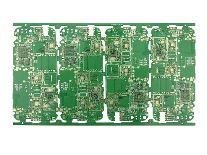
PCB高周波板の分類
Ceramic filling thermosetting material
Processing methods:
The processing flow is similar to epoxy resin/glass woven cloth (FR4), シートが脆くて簡単に壊れる以外は. 掘削とゴング, ドリルノズルとゴングナイフの寿命は.
2. PTFE (polytetrafluoroethylene) material
Processing method:
(1). Cutting material: It is necessary to save the shelter film cutting material to avoid scratches and indentations
(2). Drilling:
2.1 Use a brand new drill (size 130), 一人ずつが一番だ, the pressure of the presser foot is 40psi
2.2アルミニウムシートはカバープレートです, and then the 1mm melamine backing plate is used to hold the PTFE plate tightly
2.3掘削後, use an air gun to blow out the dust in the hole
2.4 Use the most constant drilling rig and drilling parameters (basically, 穴が小さい, 高速掘削速度, チップ負荷が小さい, the lower the return speed)
3. Via treatment
Plasma treatment or sodium naphthalene activation treatment is conducive to hole metallization
4. PTH Immersion Copper
4.1 After micro-etching (with a micro-etching rate of 20 microinches controlled), start the board from the de-oil tank in the PTH pull
4.2必要ならば, 2番目のパス, just start with the estimated cylinder and enter the board
5. Solder mask
5.1前処理:プレートの酸性洗浄を取る, and do not use machines to grind the plates
5.2 Pre-treatment and post-baking plate (90 degree Celsius, 30min), brush with green oil to cure
5.3段ベーキング:1段80, 100°C, 150°C, each for 30 minutes (if the substrate surface is oiled, it can be reworked: wash off the green oil and reactivate it)
6. Gong board
Lay the white paper on the circuit surface of the PTFE board, そして、それを厚さ1でFR - 4ベースプレートまたはフェノール性ベースプレートでそれをクランプしてください.0MM etched to remove copper:
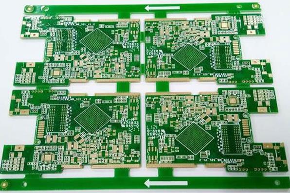
As shown in the picture: High frequency and high speed board material

When selecting the substrate used in the PCB for high-frequency circuits, 異なる周波数での材料DKとその変換特性を具体的に調べる必要がある.
高速信号伝送要件, または特性インピーダンス制御要件, 周波数のもとでのDFとその性能に対する焦点, 温湿度.
周波数変化の前提で, 通常の基板材料はDKとDF値の大きな変化の規律を示す.
特に1 MHzから1 GHzの周波数範囲で, DK値とDF値は有意に変化する.
コーティングオンラインによると, the DK value of ordinary epoxy resin-glass fiber cloth-based substrate material (ordinary FR-4) at a frequency of 1MHz is 4.

7. 1 GHzの周波数のDK値は4に変化する.19. 1 GHz以上, DK値の変化は急峻である.
その変化の傾向は、周波数の増加に続くことである, and then become smaller (but the transformation amplitude is not large), 例えば, L 0 GHzで, 通常のFR - 4のDK値は4です.15, そして、高速で高周波特性を有する基板材料は、周波数が変化する. 環境下で, DK値の変化は比較的小さい. 1 MHzから1 GHzへの遷移周波数の下で, DKはほとんど0に接続されている.02スケールトランジション.
そのDK値は、低いものから高いものまで変動する周波数の前提の下でわずかに低下する傾向があります.
The dielectric loss factor (DF) of the ordinary substrate material is affected by the frequency change (except for the change in the high-frequency scale) and the change in the DF value is greater than the DK.
その変化の規律が増加する傾向がある, したがって、基板材料の高周波特性を評価するとき, 試験の焦点はDF値変換環境である.
高速・高周波特性を有する基板材料, 高周波数での変換特性に関して通常の基板材料の2種類がある, and its (DF) value changes very little .
別のタイプは、変換振幅に関して通常の基板材料に近い, but its own (DF) value is lower.