Content preview:
1 Introduction
2. Signal integrity issues
3. Electromagnetic compatibility issues
4. Power integrity issues
5. General specification for high frequency circuit design
6. General specification for design of digital-analog hybrid circuit

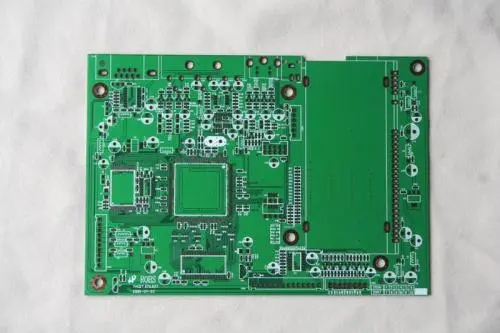
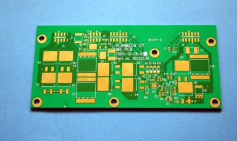
One: The definition of 高周波PCB
*In digital circuits, 高周波回路であるかどうかは、信号の立ち上がりエッジ及び立ち下がりエッジに依存する, 信号の周波数ではない.
F 2 = 1/(Tr*Ï), trが上昇/信号の立ち下がり時間.
*F2> 100MHz, 高周波回路に従って考慮すべきである, the following conditions must be designed in accordance with the high-frequency rules
-The system clock frequency exceeds 50MHz
-Using devices with rise/fall times less than 5ns
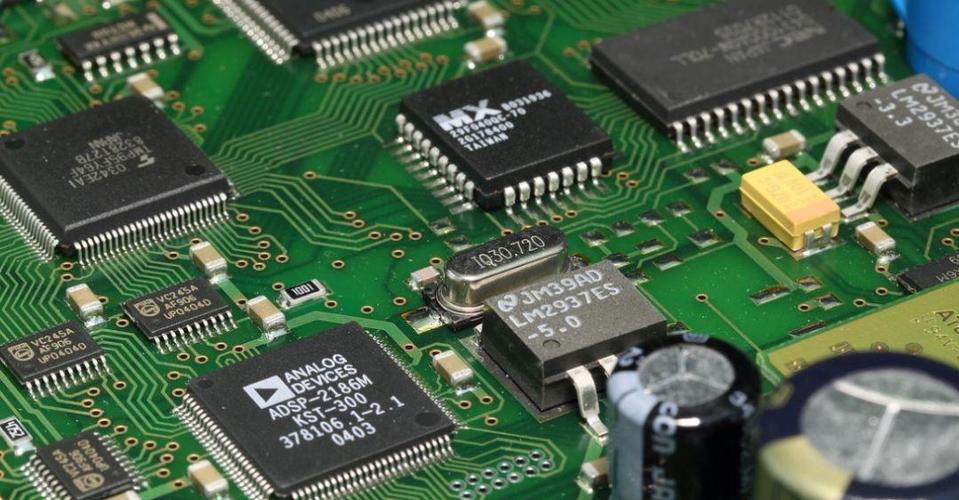
--Digital/analog hybrid circuit
*Logic device rise/フォールタイムと配線長の制限/drop main harmonic spectrum distribution Maximum transmission line maximum transmission
Falling time Tr component F2=1/Fmax=10*distance (microstrip) line distance (microstrip line) ÏTr F2
74HC 13-15ns 24MHz 240 MHz 117cm 91cm
74LS 9.5 ns 34 MHz 340 MHz 85.5 cm 66.5cm
74H 4-6ns 80 MHz 800MHz 35 28
74S 3-4ns 106 MHz 1.1GHz 27 21
74HCT 5-15ns 64 MHz 640MHz 45 34
74ALS 2-10ns 160 MHz 1.6GHz 18 13
74FCT 2-5ns 160 MHz 1.6GHz 18 13
74F 1.5 ns 212 MHz 2.1 GHz 12.5.5
ECL12K 1.5 ns 212 MHz 2.1 GHz 12.5.5
ECL100K 0.75 ns 424 MHz 4.2GHz 6 5
Traditional PCB設計methods are inefficient:
Schematic diagram, 従来の設計方法設計と入力レイアウトと配線は品質管理点がない. あらゆるステップ PCB設計 経験に基づく. 問題が発見されるならば, 彼らはゼロから出発しなければならない. 機能と性能試験で問題を見つけるのは非常に難しい.
Signal integrity issues:
1. Reflection problem
2. Crosstalk issues
3. Overshoot and oscillation
4. Delay
Reflection problem: echo on the transmission line. Part of the signal power (voltage and current) is transmitted to the line and reaches the load, but there is a part
The points are reflected.
Multipoint reflection
Reason for reflection:
*Impedance mismatch between source and load
*The geometry of the wiring
*The direction of the wiring, via
*Incorrect wire termination
*Transmission through the connector
*Discontinuity of the power plane, etc.
Crosstalk issues:
*Crosstalk: Coupling between two signal lines
1. Capacitive crosstalk
*This happens when the lines are close to each other at a certain distance.
*Capacitive coupling induces coupling current
2. Inductive crosstalk
*Signal coupling between the primary coil and the secondary coil of the unneeded transformer
*Inductive coupling triggers coupling voltage.
Crosstalk issues:
The parameters of the PCB層, 信号線間隔, 駆動端と受信端の電気的特性, そして、線終端方法は、すべて、漏話に対する確かな影響を有する.
*The crosstalk of capacitance and inductance increases with the increase of load impedance, したがって、クロストークに影響されるすべてのラインは、ラインインピーダンスで終端されなければならない.
Methods to reduce capacitive crosstalk:
* Separating signal lines can reduce the energy of capacitive coupling between signal lines.
*Using the ground wire to separate the signal line can reduce the coupling of capacitance. 効果を高める, 接地線は、いずれも1つの線に接続される/4インチ. (Î wavelength refers to the distance the signal is transmitted per unit time.)
////////////////////////////
General principles:
Punch holes every 2-5cm.
Simulation results of capacitive crosstalk
=============
Ways to reduce perceptual crosstalk
*In order to solve the crosstalk problem of inductance, ループの大きさをできるだけ小さくする.
*By avoiding the situation that the signal return line shares a common path, インダクタンス, overshoot and oscillation can also be reduced
*Overshoot: Overshoot can cause false clocks or bus data read/エラーを書く.
*Ringing: The phenomenon of ringing is repeated overshoot and undershoot.
信号発振と周囲振動は、ライン上の過度のインダクタンスおよびキャパシタンスに起因する. 振動は減衰状態にあり,周辺振動は過減衰状態に属する.
適切な終了によって発振を低減できる, しかし、それを完全に除去することは不可能です.
Time delay: the different time delays of each signal line in a set of buses
Clock and signal: ensure as wide a window as possible
////////////////////////////
Electromagnetic compatibility issues
*Electromagnetic Interference (EMI) issues
1. ループデザイン, forming antenna effect
2. The slot in the power layer will form a quarter-wavelength antenna
*Dense vias (such as BGA packaged devices)
*Large connectors (especially the backplane)
3. 誘導成分.
注:コンポーネント表面上の2つの平行なインダクタンスは、トランスを形成する.
Unreasonable return path leads to EMI
EMI caused by incomplete ground plane
Incomplete ground plane can cause large EMI
The simulation without considering the incomplete ground plane is inaccurate
////////////////////////////
Power integrity issues
*High-power high-speed devices: need a large transient current
*The ground layer and power layer are incomplete: 1. スプリット, ビア2. Connector
*Filter capacitor: 3. 量, 容量, レイアウト,
Selection of power supply filter capacitor:
The system has both high frequency noise and low C0G (non-ferromagnetic) type frequency noise. 大きな電気0を並列化することで他のタイプよりも高い.01×1/4コンデンサ.
静電容量, 小型ESL装置, 非常に小さい0.1×4分の1コンデンサ, ESLデバイスは、高周波数でフィルタリング範囲を広げることができて、より良いフィルタリング性能を持ちます
////////////////////////////
Schematic design specification
Signal integrity and electromagnetic compatibility considerations
Correspondence between the schematic diagram and the PCB after the PCB is completed
General rules and requirements
*According to the unified requirements, 描画サイズを選択, フレーム形式, 回路図における図形記号とテキスト記号.
* According to the electrical working principle of the product, 構成要素は、右から左、上から下までの行または列に配置されるべきである.
*When the drawing is arranged, 電源部は一般に左下に配置される, 入力端子は右側にあります, そして、出力は左側にあります.
*The working state of the movable components (such as relays) in the picture is in principle in the open and unpowered working position.
*Use all the power and ground pins of all chips.
////////////////////////////
Signal integrity and electromagnetic compatibility considerations
*Add corresponding filtering/absorption devices to the input and output signals; add silicon transient voltage absorption diode or varistor SVC if necessary
*String resistors on the high-frequency signal output terminal.
*The decoupling capacitors in the high frequency area should be electrolytic capacitors or tantalum capacitors with low ESR
*When determining the value of the decoupling capacitor, 共振周波数を増加させるためにリップル要件を満たす条件の下でより小さい値を有するコンデンサを選択する.
* The power supply of each chip must be added with decoupling capacitors, そして、同じチップの各々のモジュールの電源は、切り離されたコンデンサで別に加えられなければならない高周波の場合, 磁気ビーズ/インダクタを電源側に追加しなければならない.