最適化方法 PCBレイアウト to improve power module performance

The global energy shortage problem has caused governments all over the world to vigorously implement a new energy saving policy. 電子製品のエネルギー消費基準はより厳しく厳しくなっている. 電源設計エンジニア, より高い効率と高性能電源を設計する方法は、永遠の挑戦です. 電源のレイアウトから始まる PCBボード, この記事はベストを紹介します PCBレイアウト 方法, 簡単なスイッチャ電源モジュールの性能を最適化するための例と技術.
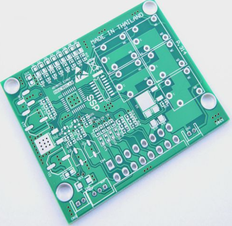
電力供給計画を計画するとき, 第1の考慮すべきことは、2つのスイッチト電流ループの物理的ループ面積である. これらのループ領域は、電力モジュール100において基本的に見えないが, それらがモジュールを越えて伸びるので、2つのループのそれぞれの現在のパスを理解することはまだ重要です. 図1に示すループ1において, the current self-conducting input bypass capacitor (Cin1) passes through the MOSFET during the continuous on-time of the high-side MOSFET to the internal inductor and output bypass capacitor (CO1), そして最後に入力バイパスコンデンサ.
ループ2は、内部ハイサイドMOSFETのオフ時間および低側MOSFETのオン時間の間に形成される. 内部インダクタに蓄積されたエネルギーは、出力バイパスキャパシタ及びローサイドMOSFET 206を流れる, and finally returns to GND (as shown in Figure 1). The area where the two loops do not overlap each other (including the boundary between the loops) is the high di/DT電流エリア. The input bypass capacitor (Cin1) plays a key role in providing high-frequency current to the converter and returning the high-frequency current to its source path.
以上が最適化方法の紹介です PCBレイアウト 電力モジュールの性能を改善する. IPCBも提供されて PCBメーカー とPCB製造技術.