PCB回路設計 and pre-production operations (basic knowledge)

1. Annular Ring
Refers to the copper ring that is flatly attached to the board surface around the wall of the through hole. 内側のボードの穴のリングは、しばしば十字橋によって外地に接続されます, そして、より頻繁に線または駅の終わりとして使われます. 外層板上, 部品ピンはんだ付け用半田付けパッドとして使用できます, 回路交差点として用いられることに加えて. There are Pad (with circle), Land (independent point) and so on that are synonymous with this word.
2. Artwork film
In the circuit board industry, この言葉はしばしば白黒の否定を指す. As for the brown "Diazo Film" (Diazo Film), また、PhotoTool. PCBで使用される否定は、オリジナルのネガティブに分けられることができます, etc.
3. Basic Grid
Refers to the vertical and horizontal grid where the conductor layout of the circuit board is designed. 初期に, 格子間隔は100ミルであった. 現在, 細い線と濃い線の流行のために, 基本的なグリッドの間隔は50ミルに削減されている.
4. Blind Via Hole
Refers to the complex 多層基板, ビアの一部は相互接続のある層を必要とするので, それで、彼らは故意に徹底的に訓練されている. つの穴が外側の板のリングに接続されるならば, デッドエンドの特別な穴を「盲目の穴」といいます.
5. Block Diagram circuit system block diagram
The assembly board and the various components required are framed in square or rectangular empty boxes on the design drawing, そして、さまざまな電気的シンボルは、一つのフレーム間の関係を通信するために使われる.
6. Bomb Sight bullet mark
Originally refers to the aiming screen where bombers dropped bombs. の否定の生産の間 PCBボード, 整列のために, 上下2層アライメント目標も各コーナーで設定される. より正確な公式の名前をフォトグラファーのターゲットと呼ぶべきです.
7. Break-away panel can be disconnected
Refers to many small-area circuit boards. プラグインの便利のために, コンポーネント配置, 下流組立ラインのはんだ付け及びその他の操作, PCB製造工程において, 彼らは特別に様々な処理のための大型ボードに結合されます. 作業完了, the method of jumping blades is used to perform a local cutting shape (Routing) disconnection between the independent small plates, しかし、十分な強さでいくつかの「タイバーまたはブレークアウェイタブ」は保持されます, 接続している. ドリルのシートとボードの端の間にいくつかの小さな穴;または、組立工程が完了した後、ボードの分離を容易にするためにV字型の切り欠きを上下する. このような小型ボードの接合方法は今後ますます多くなる, ICカードは例です.
8. Buried Via Hole
Refers to the local vias of the multilayer board. それらが多層基板の内側層の間に埋め込まれるとき, 彼らは「内部のvias」になって、外の板で「接続されません」, 埋設された潜水用または埋設されたビアと呼ばれる.
9. Bus Bar
Refers to the cathode or anode rod itself on the electroplating tank, または接続されているケーブル. 回路基板の中で, 金の指の外側の端は、板の端に近い, the original connecting wire (which must be covered during the gold plating operation), and a small narrow piece (all for saving gold (It is necessary to minimize the area) to connect with each finger. この種の導電性接続はバスバーとも呼ばれる. 個々の指がバスバーに接続されている小さな部分はシューティングバーと呼ばれています. 板が形を切ったとき, 両方とも同時に切断される.
10. CAD computer-aided design
Computer Aided Design uses special software and hardware to digitally lay out the circuit board, そして、デジタルデータを元のフィルムに変えるために光学プロッタを使用する. この種のCADは、手動式よりも回路基板の製造前工程において、はるかに正確で便利である.
11. Center-to-Center Spacing
Refers to the Nominal Distance (Nominal Distance) from the center to the center of any two conductors on the board. If the conductors arranged in a row have the same width and spacing (such as the arrangement of gold fingers), それから、この「中心から中心への間隔」もピッチと呼ばれます.
12. クリアランスルーム, クリアランス, empty ring
Refers to the inner layer of the multilayer board, 導体面が貫通孔の孔壁に接続されていない場合, 貫通孔の周りの銅箔をエッチングして、空のリングを形成することができる, 特に「空の輪」と呼ばれる. 加えて, 外側のボードと各リングに印刷された緑色のペイントの間の距離は、クリアランスとも呼ばれる. しかし, 現在の基板表面の密度が徐々に増加するため, この緑のペンキのためのオリジナルルームも、ほとんど空であることを強制されました.
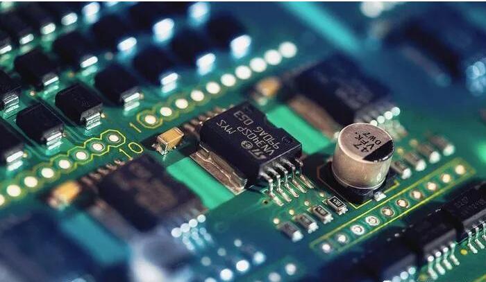
13. Component Hole
Refers to the through-holes for inserting parts on the board. このピンホールの穴径は平均約40ミリメートルです. 現在、SMTは人気になりました, 大きなアパーチャジャックの数は徐々に減少している, そして、コネクタのいくつかの金のピン穴だけは、プラグ溶接される必要があります, そして、残りのSMD部品のほとんどは表面実装されている.