IPCBは独自の SMTチップ ファクトリー, これは SMTチップ 最小パッケージにおける0201コンポーネントのための処理サービス, そして、入って来るサンプルとPCBA. 次, の影響を紹介します SMTチップ 処理. 費用率.
PCBA processing
Advantages of SMT処理
SMT processing is essentially the technology of soldering the components to the PCB light board through related machinery and equipment. 機械費は比較的大きい, それは伝統的なプラグインアセンブリと比較して独自の利点と特性を持っています. この技術には多くの利点がある, 全体的なPCBA処理効率とコンポーネントの小型化のような. 完成品ボリュームの小型化. 機械が大量に生産できるから, 労働関連規制によるコスト増加と非効率性を大いに高める, 電子製造産業全体の発展のための技術的進歩.
に含まれる主な段階 SMTパッチ処理 process
1. Solder paste printing
2. Solder paste inspection
3. Patch processing
4. Manual inspection
5. Reflow soldering
6. In (offline) AOI test
7. X-RAY detection
8. Functional test

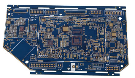
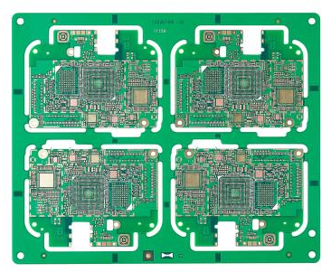
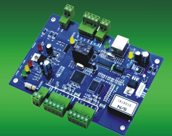
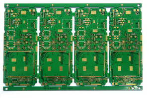
SMT processing factory
Factors affecting cost during SMTパッチ処理
1. Solder Paste Printing
The process involves placing an accurate amount of solder paste on the pads of the components to be soldered. この理由から, 半田ペーストを適切に塗布することは重要ではない, しかし、それを低温で適切に保存し、それを適用する前に室温に戻すことも重要です. 加えて, また、スクレーピング角度と速度に注意を払う必要がありますて.
2. Solder paste inspection
This step is very helpful in reducing costs, それは初期のSMTはんだ付け欠陥を見つけるのを助けるので. あなたがすることができることは、製造の後の段階で高価な欠陥を防ぐことです.
3. Patch processing
An important part of the SMT assembly process, 配置機で完了する. 小型部品は高速配置機で取り付けられるが, より大きな部品は低速で動く多機能配置機械を必要とする.
4. Manual visual inspection
The visual inspection process once again ensures that any defects can be found early. この段階で識別できるエラーのいくつかは、欠落した部分または適切な配置の欠如を含む. リフローはんだ付け後, これらの欠陥に対処するのは難しい. もう一度, SMTアセンブリのこの段階はコストコントロールを可能にする, この段階が実装されていないかのように, 後でエラーを訂正することができ、生産コストが上がる.
5. Reflow soldering
This process involves melting the solder paste so that the component can be connected to the circuit board. 温度プロファイル設定はリフローはんだ付け能力を決定し、製造コストを低減する. プロのアセンブラは大量にコストを制御できる.
6. Automatic optical inspection
At this stage, はんだ接合部の性能を十分に点検する. Some errors that can be detected at this stage include:
Tombstone, 少数の作品, 転位, ブリッジング, バーチャル溶接, etc.
7. X-ray detection
Once again, X線検査は、製品が効率的であることを保証するための良い方法であり、市販された後に製品欠陥と競合する必要がない.
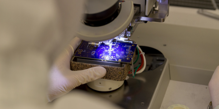
8. ICT or functional testing
Functional testing will continue to test the functions of the assembled PCB to ensure that the final product is very reliable.
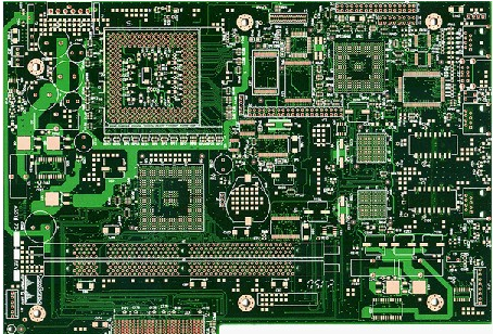
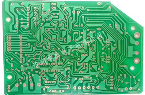
SMT processing
SMTチップ processing capability
1. The largest board: 310mm*410mm (SMT);
2. Maximum board thickness: 3mm;
3. 最小板厚:0.5mm;
4. 最小のチップ部分:0.6mm*0.3mm;
5. The maximum weight of mounted parts: 150 grams;
6. Maximum part height: 25mm;
7. Maximum part size: 150mm*150mm;
8. 最小リード部分間隔:0.3mm;
9. The smallest spherical part (BGA) spacing: 0.3mm;
10. The smallest spherical part (BGA) diameter: 0.3mm;
11. Maximum component placement accuracy (100QFP): 25um@IPC;
12. 能力を取り付けること:3/日.
なぜIPCBを選ぶのか SMTパッチ処理?
1. Strength guarantee
⪠SMT workshop: It has imported placement machines and multiple optical inspection equipment, これは、1日あたり400万ポイントを生産することができます. 各々のプロセスは、QC人員を備えています, 誰が製品の品質に目を離さない.
二段波はんだ付け機. その中で, 3年以上働いた10人以上の従業員がいる. 労働者は非常に熟練しており、すべての種類のプラグイン材料を溶接することができます.
2. 品質保証, high cost performance
⪠High-end equipment can paste precision shaped parts, BGA, QFN, 0201材料. また、手でバルク材料を実装し、配置するためのモデルとして使用することができます.
両方のサンプルと大きくて小さいバッチは、生産されることができます. 証明は800元で始まる, そして、バッチは0から始まります.008元/ポイント, スタートアップ料金はない.
3. 電子製品のSMTとはんだ付けにおける豊富な経験, stable delivery
⪠Accumulated services to thousands of electronic companies, 関与 SMTチップ 様々な種類の自動車設備および産業用制御マザーボードのためのプロセシングサービス. 製品はしばしばヨーロッパと米国に輸出される, そして、品質は新しいと古い顧客によって肯定されることができます.
タイムオンデリバリー, 通常の3 - 5日後に材料が完了した, また、小さなバッチは、同じ日に出荷することができます.
4. Strong maintenance ability and perfect after-sales service
⪠The maintenance engineer has rich experience and can repair the defective products caused by all kinds of patch welding, そして、各回路基板の接続率を確保することができます.
24時間カスタマーサービススタッフは、いつでも応答し、できるだけ早くあなたの注文問題を解決します.