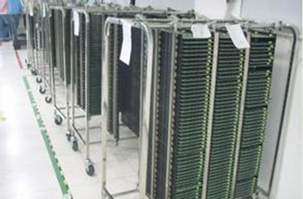
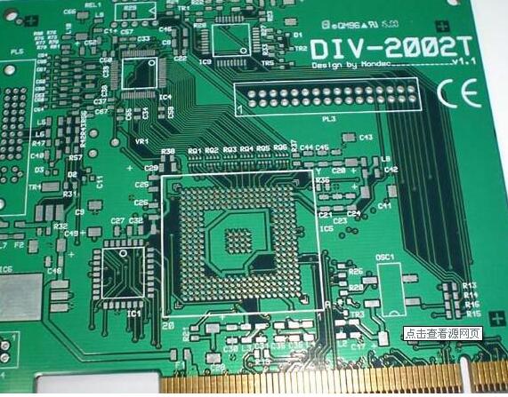
PCB技術 copper clad laminate raw material
The supply chain pattern of special electrolytic copper foil, 特殊樹脂, 新・ハイエンド用の特殊ガラス繊維 基質材料, and the new パフォーマンス requirements for these three major materials
This article describes the supply chain pattern of special electrolytic copper foil, 特殊樹脂, 新・ハイエンド用の特殊ガラス繊維 基質材料 近年, だけでなく、これらの3つの材料の新しいパフォーマンス要件.
2020年の初め以来、新王冠の流行の世界的な広がりは、私の国の銅張積層材の需給チェーンの深刻な変化を引き起こしました。5 g,高周波・高速回路用銅張積層板の開発以来,高hdi,ic実装基板用基板材料も,技術,性能,品種に大きく進化してきた。これらの2つの重要な変化に直面して、電子銅箔、特殊樹脂および特殊ガラス繊維布の供給チェーンパターンに関する詳細な研究は、3つの主要な材料のための新しい性能要件と同様に、新しいと高エンドの基板材料で使用される、非常に重要な、緊急に必要な仕事と見なされます。本稿ではこれら2つの側面を論じた。
電解銅箔
1.1 The current supply of various low-profile electrolytic copper foils and the new characteristics of the market structure
The scale and pattern of the global high-frequency and high-speed electrolytic copper foil market in 2019 (market share of each country/region and major manufacturers) are shown in Figure 1 and Table 1.
( Wechat ImageCell 20201028142441 ).png
Figure 1 The scale and pattern of the global 低姿勢銅箔 market in 2019
Table 1 Statistics and forecast of the market structure of low-profile copper foil for high-frequency and high-speed circuits in 2018 and 2019
WeChat image_20201028142508.png
From Figure 1 and Table 1, it is known that the global production and sales volume of low-profile copper foil (ie market size) is estimated to increase by 49.2019年の8 %, 到達,000トン. それは7を説明すると推定されます.全世界電解銅箔の6 %. 2019年の世界的な高周波および高速電解銅箔製造と販売の間で, the ratio of RTF to VLP+HVLP production and sales is approximately 77:23. しかし, the proportion of VLP+HVLP will increase in the next few years.
2019年, 中国本土で生産された国内外の銅箔企業,低プロファイル銅箔580トン, 国内資金企業が51を占めた.2% (3880 tons). 国内産企業による低プロファイル電解銅箔の製造・販売は2件を占めた.7% of the total output (144,000 tons) of copper foil for electronic circuits in domestic-funded enterprises. 2019年, domestic domestic-funded enterprises achieved new breakthroughs in mass production of VLP+HVLP varieties, しかし、そのような低姿勢銅箔の生産と販売は非常に小さい, わずか2会計.そのような電解銅箔の全世界的な生産と販売の3 %.
1.2 New characteristics of differentiation of low-profile electrolytic copper foil varieties and performance requirements for high-frequency and high-speed circuits
1.2.1 Corresponding to different transmission loss grades of high-frequency and high-speed copper-clad electrolytic copper foil varieties and low profile
In order to pursue better signal integrity (Signal Integrity, abbreviated SI) for high-frequency and high-speed circuits, copper clad laminates must achieve (especially at high frequencies) lower 信号伝送損失 performance. これは、銅張積層銅箔の製造に使用される導体材料を必要とする, 低特性の特徴. それで, 銅張積層板の製造に使用される銅箔は、低Rz, 低RQと他の品種.
信号伝送損失の4つのレベルによると, 種々の低姿勢銅箔品種に対応, RZ要件と主要メーカーのブランド, 表2に示すとおり. 表2はまた、必要な量の基板透過損失グレード銅クラッド積層材の様々なタイプの低プロファイル銅箔の順位付けを示す.
Table 2 Rz index range of several electrolytic copper foils corresponding to different transmission loss grades of high-frequency and high-speed copper clad laminates
1.2.2 The performance difference of low profile electrolytic copper foil in different application fields
The varieties of low-profile electrolytic copper foils for high-frequency and high-speed circuits are divided into five categories according to application fields. それで, 硬質無線周波用低プロファイル電解銅箔/マイクロ波回路高速デジタル回路用の低姿勢電解銅箔フレキシブルのための低姿勢電解銅箔 PCBs基板を実装するための低プロファイル電解銅箔厚い銅のための低姿勢電解銅箔 PCB 銅箔. これらの5つのアプリケーション領域で, 高周波および高速回路用の低プロファイル電解銅箔は、性能要件に関して異なる特性を有する, それで, 彼らはパフォーマンスの項目に焦点を当てており、パフォーマンス指標の異なる.
The performance requirements and differences of low-profile electrolytic copper foil varieties used in the five major application fields are shown in the following aspects:
(1) Low profile electrolytic copper foil for rigid RF/microwave circuits
Low-profile electrolytic copper foil for rigid RF/マイクロ波回路は異なる印加周波数条件の下でより明白な相対的な違いを持つ. 要求は、基板のDk均一性に関する銅箔性能に関してより厳しい, signal transmission loss, 処理層には強磁性元素はない, and PIM (Passive Inter-modulation).
この理由から, copper foil used in high-end RF-microwave circuit substrates (such as millimeter-wave automotive radar substrates) generally requires pure copper treatment to support the reduction of passive intermodulation (PIM) and realize the improvement of copper clad laminates. 低PIM性能, 参考指数:下に達する. 銅箔処理層は砒素フリーである.
同時に, このタイプの銅箔の異なる樹脂基板のため, 異なるRZ銅箔品種の選択には大きな違いがある.
硬質無線周波用低プロファイル電解銅箔/マイクロ波回路は、一般に18, - 35センチメートル, 銅箔厚さ仕様の70〜1 / 4 m, ハイエンドの超低または超低姿勢銅箔が厚さ仕様で広く使われる間、9, 12センチメートル, 18匁1 , 000 m品種 .
(2) Low-profile electrolytic copper foil for high-speed digital circuits
In the application market of low-profile copper foil for high-speed digital circuits, most of them are positioned at frequencies generally in the centimeter wave (3ï½30GHz) range. メインアプリケーション端末はハイエンドサーバです. この種の銅箔の性能は、基板の挿入損失及び基板の加工性に重要な影響を及ぼす, そして、このための厳しい要件があります. 同時に, 銅箔の薄い仕様と低コストも重要な要件である. 高速デジタル回路用の低プロファイル電解銅箔は一般的に18, - 35センチメートル, 銅箔厚さ仕様の70〜1 / 4 m, ハイエンドの超低または超低姿勢銅箔は、厚さ仕様で主に使用されるが, 12センチメートル, そして18.
The author has investigated and compared the contours of the non-pressing surface of many low-Rz copper foil varieties (including HVLP, VLP, RTF, etc.), そして、派生した結論は:同じ等級, Siプロパティでより良いパフォーマンスを得る品種について, their non-compression surface profile (expressed in Rz or Ra) is generally low. 例えば, 前金の企業のRTF銅箔製品のために, そのRZ = 3.0μm (typical value), 非加圧面はRZ=3である.5センチメートル. したがって, それがRFであるかどうか/マイクロ波回路基板または高速デジタル回路基板, より良いSi性能を追求するために, they also need the Rz (or Ra, Rq) of the non-pressing surface of the first profile copper foil, また、非常に低いプロファイル.
現在, an important category of low-profile copper foil for high-speed digital circuits is reversed copper foil (RTF). 近年, 日本と台湾の銅箔企業によるRTF銅箔技術の進歩, RZが2未満の多くの種類.5 , 000分の1 mが出ている, さらにRZが2未満の品種でも.0 , 000分の1 mが現れた. このように, その応用市場と高速デジタル回路用のグローバル低姿勢銅箔市場の割合も急速に拡大している.
現在, グローバル銅箔の低姿勢電解銅箔製造工業は剛性RF用銅箔で同じ性能に向かっている/高速ディジタル回路用のマイクロ波回路と銅箔. 例えば, CircuitFoil (CircuitFoil) realized mass production of ultra-low profile copper foil BF-NN/2019年のBF‐NN‐HT. この品種は「二つの互換性」を達成しました, オリジナルのBF - ANP銅箔はPTFE樹脂タイプの基板にのみ使用される, and it has developed to "including polyphenylene ether (PPE/PPO)-based resin systems. It is also suitable for pure Or modified fluoropolymer (PTFE) resin system.■, 無線周波数マイクロ波回路基板に適用でき、高速デジタル回路基板にも適している.
(3) フレキシブルのための低姿勢電解銅箔 PCB
低プロファイル電解銅箔をフレキシブルに使用 PCBs. 微細回路製造のために, ultra-thin copper foil (without carrier) is often used. このタイプの製品の現在の最小厚さ仕様は、6, 福田金属箔のCF - T 4 X - SV 6とCF - T 49 A - DS - HD 2のような., Ltd.; 三井金属(株)., Ltd. ((最小厚さは7×1 / 4 m)) .
Low profile electrolytic copper foil for flexible PCB また、高い引張強さと高い伸びを有する銅箔が必要である. エッチング後のベースフィルムの優れた透明性もこの銅箔市場の重要な要求事項である.
フレキシブルのための高周波低姿勢電解銅箔 PCBsは近年、低姿勢になり始めた. RZが1未満の多くの品種.業界には0 %が現れた. 例えば, 三井金属TQ - M 4 - VSP RZ.6 (typical value); Foton Metals CF- T4X- SV Rz=1.0 (typical value, 仕様9/12/18); Foton Metals CF- T49A- DS- HD2, RZ = 1.0 μm (typical value) (specification 6/9/12/18); Nissin ISP, RZの.55 (typical value).
(4) Low profile electrolytic copper foil for IC package carrier board
The low-profile electrolytic copper foil required for the package carrier (including the module substrate) should have high tensile strength, 高い熱安定性, 高弾性率, and high peel strength at high temperatures (after 210°C/1時間 treatment). 厚さ仕様は5です.0・1・1・1・1・2・12・1・1・4 m. 近年, ハイエンドICパッケージング基板用銅箔の厚み仕様は、より薄くなるように発展している, それで, 厚さは1に達する.5・1・1・3・1・1・4 m.
Package carrier boards (including module substrates) have also seen demand for high frequency and high speed 近年. したがって, in recent years, パッケージキャリア用の低プロファイル電解銅箔の種類が多く登場. 例えば: Mitsui Metals' 3EC-M2S-VLP (without carrier), RZの.8 μm (typical value); after 210 degree Celsius/1h, 引張強さは/mm 2伸び率は4である.6 %;銅箔の最も薄い仕様は9. Mitsui Metals' MT18FL (with carrier), RZの.- 3, 回路銅箔の仕様は1である.5, 2, - 3. The LPF (without carrier) of Nissin Material Co., Ltd., RZの.72 (typical value), 210度後の引張強さ/1 hは52です.3 kgf/MM 2伸びは3である.7 %;銅箔の最も薄い仕様は9.
(5) 高電流厚銅用の低姿勢電解銅箔 PCB

Low-profile electrolytic copper foil for 高電流厚銅PCB with thickness specifications â¥105um (3oz). 一般的な仕様:105, 140, 175, 210匁1 , 000分の1. 特殊な厚さの要件を有する超厚電解銅箔もある, with thickness specifications up to 350μm (10oz) and 400μm (11.5oz).
高電流厚銅用の低姿勢電解銅箔 PCBs is mainly used for the manufacture of high-current, 電源基板, 高放熱回路基板. 厚い銅 PCB 製造は主に自動車エレクトロニクスで使用される, 電源, ハイパワー工業用制御装置, 太陽設備, etc. 近年, の熱伝導率 PCB は、最も一般的で重要な機能の一つとなっている. 超厚銅箔の市場需要は常に拡大している. 同時に, 厚肉銅のマイクロ回路製造技術の開発と応用により PCB, また、使用する必要がある超厚銅箔は、低プロファイル特性を有する. For example, Mitsui Metals RTF type low profile thick copper foil: MLS-G (Type II), RZ = 2.5μm (product typical value). リュクサンブール, RZの値.2μm (product index).
1.3 Application market expansion and performance requirements of ultra-thin electrolytic copper foil for IC package substrates
A recent paper written by an overseas PCB 専門家は、超薄のアプリケーション市場とアプリケーション性能要件について、より鋭い説明をしました, low-profile copper foil. 記事は前向きに述べます, HDIボードは、IC基板製品で一般的に使用されている多数の回路電気めっきプロセスを使用し始めた. This process is called semi-additive process (SAP), 電気めっき技術. ICキャリアボードの回路構成の要件を満たすために, このプロセスは一般的なHDIボードでは採用されていない. しかし, after the adjustment of semi-additive technology (mSAP) with ultra-thin copper skin, HDI製造の主流プロセスとなっている.