PCB プロセス ホットバー design can not be ignored
Hot-Bar reflow (melting tin hot pressure welding), its most important function is to use the hot press head to melt the solder paste that has been printed on the electronic printed circuit (PCB), つの独立した電子部品を接続するために. The method is to solder the flexible flat cable (FPB) to the electronic printed circuit (PCB).
ホットバーマシンのホットプレスヘッドが唯一の熱源から, when the hot pressing head is pressed on the flexible flat cable (FPC), 熱は電子に下向きに転送しなければならない プリント回路基板(PCB) to melt the printed circuit on the electronic printed circuit The solder paste on the board, したがって、フレキシブルフラットケーブルは、熱伝導性の設計をしなければならない.
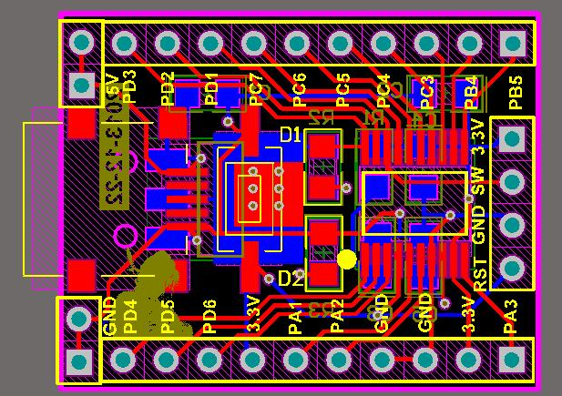
一般的に言えば、以下の図に示すように、半田パッドにめっき孔またはビアを作ることは、最も一般的な熱伝導機能設計である。それぞれのFPCの半田パッドに3つのビアまたは2.5ビアを持つことを推奨します。また、電気メッキ孔を作る利点もある。溶融錫のホットプレス溶接時には、電気めっきされた孔から余分な錫をオーバーフローさせることができ、半田パッド間に短絡を生じさせない。
フレキシブルフラットケーブルは、フレキシブルプリント配線を固定するために、電子テープ基板上にフレキシブルフラットケーブルを固定する必要がある。また、不安定な品質の問題も生じることがある。
fpcの設計要件を要約する。各々のFPCの半田パッド、少なくとも2つの+半分のメッキされた穴またはバイアホールの上に、3つのメッキされた穴またはヴィアホールがある方がよいです。

Stick double-sided tape on the side of the flexible flat cable (FPB) that is attached to the electronic プリント回路基板. 両面テープの厚さは0以下でなければならない.15 mm, との距離からの距離 FPC 両面テープへのパッドは0でなければなりません.20 mm. 距離.
推奨 ホットバー size design is as follows:
The aperture of the via hole is 0.4mm
Through hole center to center is 1.2mm
The distance from the center of the pad to the center is 1.8mm
The pad width is 0.9 mm
フレキシブルフラットケーブルの破壊による応力集中を避けるために、フレキシブルフラットケーブルのカバーフィルム(ポリアミド)の端を引っ張ることが強く推奨される。
ホットバーの操作に協力し、部品のプレスまたは破損を避ける, the following is the recommended limit size of the parts:
The minimum dimension from the part to the front edge of the FPC は2です.0 mm.
左と右端の部分の最小サイズ FPC は3です.0 mm.
時 FPC が拡張される, 最小5のスペース.0 mmのために0 mmを予約しなければならない FPC に貼り付けることができます プリント回路基板. また、位置決め穴を作ることもできます FPC, and designing alignment pins (Alignment Pins) on the hot press fixture for positioning, 両面テープでスペースを節約できます プリント回路基板, しかし、精度を考慮する必要があります.
下の部分の最小サイズ FPC to the rear edge of the FPC 10です.0mm (in order to ensure that the double-sided adhesive can be pasted on the プリント回路基板).