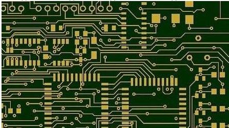
電路板設計 規範厚銅板設計規範
對於銅厚度超過2盎司的印刷電路板電路板,由於銅厚度,電路板設計規範不同於一般電路板。 為此,該公司專業為厚銅板指定了檔案檢查規範,以便客戶能够提供更優質的電路板。
1:電線設計規範 電路板 design
A: The minimum wire width of the 電路板 不小於0.3mm;
B: In general, 相鄰導線之間的距離不應小於0.25毫米
C: The copper foil around the fixing hole is not less than 0.距孔邊緣4mm; 不應有細導線1.5毫米 from the edge of the hole
E: Whether to consider low-density wiring design
F: Whether the wires are laid out according to the shortest route, and whether there will be no sharp angles at the turn
G: Whether the junction between the wire and the pad is smoothed into a slope
H: In the power circuit, the distance between adjacent wires between hot and cold ground should not be less than 6mm
I: The distance between the wire and the edge of the printed board is generally not less than 3mm, 尤其是不小於1.5毫米, 但佈線寬度不得小於1.5毫米; 接地線不得小於0.5mm

2:電路板設計用焊盤設計規範
A: The distance between the pad of the interposing component and the edge of the printed board is generally not less than 7mm, 尤其是不少於3.5mm. The distance between the pad and the edge of the mounted component should not be less than 5mm; The physical and pad distance of the interposing component or the mounting component should not be less than 5mm from the edge of the board
B: For ICs with a 1.78mm銷間距, the connection (pad) pitch should not be less than 0.3mm
C: The minimum diameter of the circular pad, whether it meets the standard
D: After the wave soldering of the components inserted, whether the pads are driven away from the tin bath
E: There must be no connection between the pads, between the pads and the exposed copper foil
F: Whether the pads of the switching transformer and the harmonic current suppressor are removed from the empty pads to prevent mis-insertion
G: The filter inductance of the AC input circuit, 開關變壓器的襯墊是否, 逆變變壓器, 大功率電阻器, high-power damping or rectifier straddle diode (non-plastic package), and rectifier large electrolytic capacitor are reinforced with rivets
H: The number of rivet pads of multi-pin component pads, 一般不應小於1/2 of the number of pins of the component
I: Whether the design requirements of the rivet hole pad meet the standard; the rivet pad with a 1.8mm孔徑為4.5mm. 如果不符合要求, a 4.必須使用0毫米的襯墊,並且需要一個水滴狀的上錫加强件. 鉚釘墊帶有2.4mm孔徑為5.5mm, 如果不滿意, 使用5.0mm pad and add drop-shaped upper tin reinforcement
J: Take the printed board positioning hole as the center, 在7mm半徑內未設計鉚釘墊, and rivet pads are not designed for adjacent holes with a distance of less than 6mm
H: Whether the key components are reinforced with rivets, and whether the pads of the key components are tinned with water droplets
3:電路板設計的熱設計規範
A: Whether the thermal element is far away from the heat sink
B: Are there heat dissipation measures for high-power components?
C: The distance between the high-power heating device and the large-volume electrolytic capacitor must be greater than 5mm
D: Have you considered the heat conduction facilities of the device?
E:散熱器的固定和位置是否合適?
F:加熱裝置應在相應的印製板下方和周圍有適當數量的散熱孔, and the diameter is generally not greater than 4mm
G: Large-area copper foil is easy to be heated to produce copper foil expansion, 面積超過15mm圓的直徑, the conductive layer must be opened with a conductive window
4:電路板設計的佈局設計規範
A: Is it possible to complete production through the simplest assembly process?
B:大功率器件的佈局是否均勻, 是否考慮散熱流向, and the board strength
C: Is the fixing device added to the high-quality device?
D:你考慮過設備的絕緣措施嗎?
E: Whether the arrangement of components is horizontal or vertical
F: The radiator must not touch the surrounding components
G: Whether the design of the cushion position is evenly distributed
H: Whether there are nail bottom components and flying leads
I: Whether the heat sink installation complies with the heat dissipation flow direction, and whether to use the existing heat sink as much as possible to reduce the possibility of making a new heat sink
J: Whether the maximum 印刷電路板板 長度不超過600mm, and the width is not more than 360mm
K: Are there grounding lugs at the fixed holes for cold ground installation? 接地片是否足够?
五十:電路板銅箔表面是否有3個以上的全域標記點, and whether the increased position meets the process requirements and affects the safety distance
M: Whether the arrangement of the vertical electrical plug-in components can ensure that the outer edge distance between the pieces is more than 1mm
N: Whether there are solder pads and copper foil on the edge of the printed board, making assembly more difficult
O: Whether the vertical board considers the fixing method
P: Whether the components fixed on the heat sink leave a space that can be disassembled without disassembling the heat sink
Q: Are there tall and dense components or sharp radiator corners around the power strip?
R: Whether the placement position of the input and output power strips meets the convenience of connecting with other boards of the whole machine
S: Whether the SMD components are placed perpendicular to the long side of the board to avoid fracture or damage due to deformation
T: Whether the plug-in IC and the chip IC are placed horizontally and the direction of the wave soldering is consistent with the wave soldering process, and whether the IC is designed with tin-theft pads in the appropriate position during the wave soldering to avoid continuous soldering of the soldering pads
U: Whether to consider avoiding shadow effects when placing all SMD components
V: Is there any positional interference between the screws of the fixed components and the radiator and the components on the board?
5:焊接設計規範 電路板 design
A: Whether there is a 3mm wide reserved bracket position in the middle of the 印刷電路板 board that is wider than 180mm or longer than 320mm through wave soldering
B: The reserved position of the support bar should not be within the bending range of the component lead
C: Components that are not suitable for wave soldering due to structural limitations, 需要在波峰的相反位置添加錫槽, 槽寬為0.7mm
D: The direction of wave soldering needs to be clearly marked on the upper and lower sides of the board
E: Try not to lay out components like horizontal plug-in wires that extend out of the edge of the board.
F:電力插頭部件導線的彎曲, 3極管周圍的區域, IC和插座引腳墊, should be coated with a secondary solder mask
G: A large area of copper foil is easy to be heated to produce copper foil expansion, 囙此面積超過了15mm圓的直徑, 導電層需要打開一個導電視窗或柵極