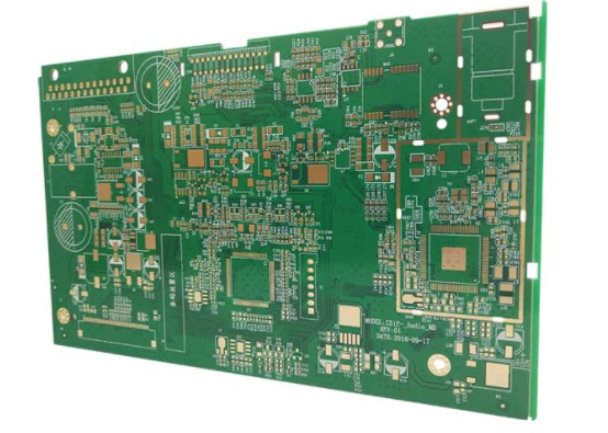
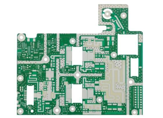
定義 高頻板 對於 <一 href="/tw/" target="_self">電路板 生產高頻板是指 電路板 電磁頻率較高, which is used for high frequency (frequency greater than 300MHZ or wavelength less than 1 meter) and microwave (frequency greater than 3GHZ or wavelength less than 0.1 meter). 印刷電路板是 電路板 在微波基覆銅板上採用普通硬質合金部分工藝生產 電路板 製造方法或使用特殊加工方法. 一般來說, a 高頻板 可以定義為 電路板 頻率在1GHz以上!

隨著科學技術的飛速發展, more and more equipment is designed for applications in the microwave frequency band (>1GHZ) or even in the millimeter wave field (30GHZ). 這也意味著頻率越來越高, 以及 電路板 是對資料的要求越來越高. 例如, 基板資料需要具有優异的電力效能, 化學穩定性好, 並且隨著功率訊號頻率的新增,襯底上的損耗很小, 因此 高頻板 突出顯示. 2. PCB高頻板 應用領域:移動通信產品; 功率放大器, 低雜訊放大器, 等.; 功分器等無源元件, 耦合器, 雙工器, 篩檢程式, 等.; 汽車防撞系統, 衛星系統, 無線電系統, 和其他欄位, 電子設備的高頻化是發展趨勢.
2. PCB高頻板 應用領域:移動通信產品; 功率放大器, 低雜訊放大器, 等.; 功分器等無源元件, 耦合器, 雙工器, 篩檢程式, 等.; 汽車防撞系統, 衛星系統, 無線電系統, 和其他欄位, 電子設備的高頻化是發展趨勢.
的分類 高頻板 powder ceramic filled thermosetting 材料
A. Manufacturer:
4350B/4003C from Rogers
Arlon's 25N/25FR
Taconic's TLG series
B. Processing method:
The processing process is similar to epoxy resin/glass woven cloth (FR4), 但板材相對易碎,容易斷裂. 鑽孔和敲鑼時, 鑽頭和鑼刀的壽命降低20%. PTFE (polytetrafluoroethylene) 材料
A. 製造商:RO3000系列, RT系列, TMM series from Rogers
Arlon's AD/AR系列, IsoClad系列, CuClad series
Taconic's RF series, TLX系列, TLY series
Taixing Microwave's F4B, F4BM, F4BK, TP-2
B. 處理管道:1. Cutting: The protective film must be kept for cutting to prevent scratches and creasing
2. Drilling
1. Use a brand new drill tip (standard 130), 一個接一個是最好的, the pressure of the presser foot is 40psi
2. 鋁板是蓋板, and then the PTFE plate is tightened with a 1mm melamine backing plate
3. 鑽孔後, use an air gun to blow out the dust in the hole
4. Use the most stable drilling rig and drilling parameters (basically the smaller the hole, 鑽孔速度越快, 晶片負載越小, the smaller the return speed)
3. Hole treatment
Plasma treatment or sodium naphthalene activation treatment is conducive to hole metallization
4.PTH copper sink
1 After the micro-蝕刻 (the micro-etching rate has been controlled by 20 microinches), in the PTH pull from the de-oiler cylinder into the board
2 If necessary, 通過第二個PTH, just start the board from the expected cylinder
5. Solder mask
1 Pre-treatment: Use acidic plate washing instead of mechanical grinding plate
2 Baking plate after pretreatment (90 degree Celsius, 30min), brush with green oil to cure
3 Baking plates in three stages: one section of 80 degree Celsius, 100攝氏度, 150攝氏度, each for 30 minutes (if you find that the substrate surface is oily, you can rework: wash off the green oil and reactivate it)
6.Gong board
Lay the white paper on the circuit surface of the PTFE board, 然後用 FR-4基板 或厚度為1的酚醛基板.0毫米蝕刻以去除銅, 如圖所示: 高頻板 lamination method
The burrs on the back of the 鑼板需要手動仔細修整,以防止損壞基板和銅表面, 然後用相當大尺寸的無硫紙分離, 並進行目視檢查. 减少毛刺, 關鍵是 鑼板 流程必須有良好的效果.
四是工藝流程NPTH的PTFE板材加工流程
Cutting-Drilling-Dry Film-Inspection-Etching-Erosion Inspection-Solder Mask-Characters-Spray Tin-Forming-Testing-Final Inspection-Packaging-Shipment
PTH's PTFE plate processing flow
Cutting-drilling-hole treatment (plasma treatment or sodium naphthalene activation treatment)-copper immersion-board electricity-dry film-inspection-diagram electricity-etching-corrosion inspection-solder mask-character-spray tin-molding-test-final Inspection-Packaging-Shipping Five
V. 總結的困難 高頻板 processing
1. Immersion copper: the hole wall is not easy to be copper
2. 地圖傳輸線隙和沙眼的控制, etching, line width
3. 綠油工藝:綠油附著力, green oil foaming control
4. 各工序嚴格控制板面劃痕.