在裡面 PCB佈局 設計, 除了考慮自身接線問題外, 還應考慮一些隱藏的問題. 這些問題在設計時並不明顯, 但是解决這些問題很麻煩. 這是電路干擾的問題.

在 PCB設計 過程, 只有瞭解一些設計基礎知識才能解决簡單和低頻的問題 PCB設計 問題, 但對於複雜的高頻訊號,這要困難得多 PCB設計. 解决設計未仔細考慮的問題通常需要很多時間, 它甚至可能被重新設計. 因此, the following problems should be solved in the design of the PCB:
Thermal interference and resistance of advanced PCB設計
部件在運行過程中有一定的熱量, 尤其是功率更大的設備發出的熱量會干擾周圍的溫度敏感設備. 如果熱干擾沒有得到很好的抑制, 整個電路效能的電力將發生變化.
共阻抗和先進的抑制 PCB設計
公共電阻干擾是由電路上的大量地線引起的 PCB板. 當兩個或多個回路共用一段接地線時, 不同的回路電流將在共亯地線上產生一定的電壓降. 該壓降在放大時會影響電路效能; 當電流頻率很高時, 它會使電路受到大電感的干擾.
先進電磁干擾及其抑制 PCB設計
電磁干擾是由電磁效應引起的干擾. 由於PCB上的組件和佈線越來越密集, 如果設計不當,會產生電磁干擾.
印刷線路的寬度和間距 PCB設計 rules
The width and spacing of printed wires, 通常導線的最小寬度為0.5-0.8mm, 間距不小於1mm.
(1) The minimum width of the printed wire: It is mainly determined by the adhesion strength between the wire and the insulating substrate and the current value flowing through them. 由於大電流, PCB的電源線和地線在設計時應適當加寬, 一般不小於1mm. 用於低安裝密度的PCB, 印刷導體的寬度最好不小於0.5毫米. 手工板不得小於0.8mm.
(2) Printed conductor spacing: determined by the safe working voltage between them. 相鄰導線之間的峰值電壓, 基板的質量, 表面塗層, 電容耦合參數都會影響印製線路的安全工作電壓.
PCB設計 rules for printed wiring wiring
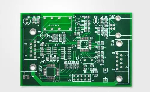
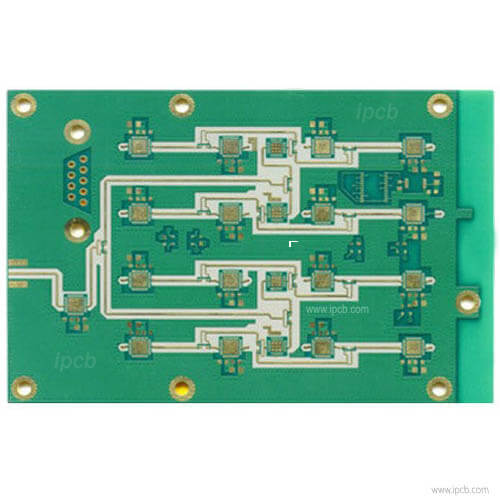
Wiring refers to the placement of the direction and shape of printed wires. 這是 PCB設計, 這是工作量最大的一步. PCB佈線包括單面佈線, 雙面佈線和多層佈線; 還有兩種接線管道:自動接線和手動接線.
在裡面 PCB設計, 為了獲得滿意的佈線效果, the following basic principles should be followed:
1) The direction of the printed line-take it as straight as possible, 最好是短的, 不要走得太遠.
2) The bending of the printed line-the routing is smooth and natural, 連接是圓形的, 避免直角.
3) Printed wires on the double-sided board-the wires on both sides should be avoided to be parallel to each other; the printed wires used as the input and output of the circuit should be avoided as much as possible, 最好在這些導線之間加一根接地線.
4) The printed wire is used as a ground wire-keep as much copper foil as a common ground wire as much as possible and arrange it on the edge of the PCB.
5) The use of large-area copper foil-it is best to hollow out into a grid during use, 有利於消除銅箔和基板之間的粘合劑加熱產生的揮發性氣體; 當導線寬度超過3mm時, 中間留有凹槽,便於焊接.
組件的間距和安裝尺寸 PCB設計 rules
It is about the spacing between the elements and the size of the installation during the layout of the components in the PCB設計.
(1) Pin spacing of components: Different components have different pin spacing. 但是對於所有類型的組件, the pin spacing is mostly: 100mil (English) integer multiples (1mil=l*10(-3 cubic)in=25.4*10(-6th power)m), 100mil通常被視為1節距. 在 PCB設計, 必須準確說明部件的銷間距, 因為它决定了焊盤放置間距. 確定非標準設備銷間距的最直接方法是使用遊標卡尺量測.
Pin spacing of common components a) DIP IC b) TO-92 type three pole tube c) 1/4w type resistor d) a trimming resistor
(2) The installation size of the components: the solder hole pitch is determined according to the pin pitch. 它有軟尺寸和硬尺寸. 軟尺寸基於其銷可以彎曲的組件, 囙此,這種裝置的焊錫間距設計更加靈活; 而硬尺寸是基於其銷不能彎曲的組件, 焊接間距要求相當準確. 設計PCB時, 元件的焊孔間距可以通過CAD軟件中的校準工具確定.
組件的佈置 PCB設計 rules
The arrangement of the components on the PCB can be one of three arrangements: ir有規律的, regular, 和網格, 或同時多個.
(1) Irregular arrangement: The axis directions of the components are inconsistent with each other, 便於印刷線路的佈置, 平面利用率高,分佈參數小, 這對高頻電路特別有利.
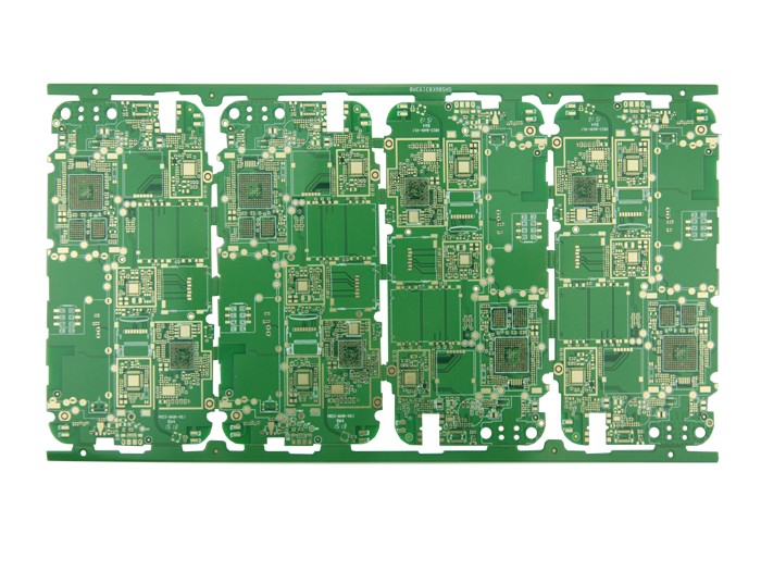
(2) Regular arrangement: The components are arranged in the same axial direction, 佈局美觀整潔, 但是接線又長又複雜, 適用於低頻電路.
(3) Grid arrangement: each mounting hole in the grid arrangement is designed at the intersection of the square grid.
The layout of the components of the PCB layout design rules
The layout methods of the components of the PCB設計 規則包括:組件佈局要求, 組件佈局原則, 組件佈局順序, 和常用組件的佈局方法.
印刷電路板內佈局, 當我們使用Protel時, DXP, 墊, Protel DXP等繪製電路板的工具, we need to pay attention to the following aspects
(1) Component layout requirements: ensure circuit functions and performance indicators; meet the requirements of processability, 測試, 維修, 等.; 部件排列整齊, 密集, 和美學.
(2) The principle of component layout: The arrangement direction should be as consistent as possible with the schematic diagram, 接線方向應與電路圖的接線方向一致; PCB周圍有5-10mm的間隙,無法放置元件; 部件的佈置應有利於加熱部件的散熱; 在高頻下, 應考慮組件之間的分佈參數. 通常地, 電路應盡可能並聯佈置; 高壓和低壓應隔離. 隔離距離與耐受電壓有關. 對於單面PCB, 每個元件引脚佔用一個唯一的焊盤, 組件不能上下交叉, 兩個相鄰部件之間應保持一定距離, 它們不應該太小或太過觸碰.
(3) Layout order of components: place the components with a larger area first; integrate first and then separate; first main and then second, 在多個集成電路的情况下,首先放置主電路.
(4) Layout method of common components: adjustable components should be placed on the printed circuit board for easy adjustment; components with a mass of more than 15g should use brackets, 大功率組件應安裝在整機底盤底板上. 敏感部件應遠離加熱部件; 對於管狀部件, 它們通常水准放置, 但當PCB尺寸不大時, 它們可以垂直放置. 垂直放置時, 兩個襯墊之間的距離通常為0.1-0.2 in(1 in="25" 4*10 (-3 cubic) m); For integrated circuits, 有必要確定定位槽的方向是否正確.