Content preview:
1 Introduction
2. Signal integrity issues
3. Electromagnetic compatibility issues
4. Power integrity issues
5. General specification for high frequency circuit design
6. General specification for design of digital-analog hybrid circuit

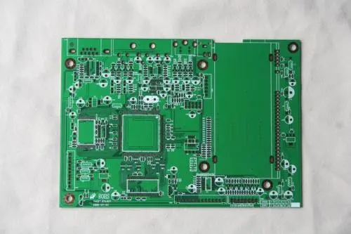
One: The definition of 高頻PCB
*In digital circuits, 它是否為高頻電路取決於訊號的上升沿和下降沿, 不是訊號的頻率.
公式:F2=1/(Tr*Ï), Tr是上升/訊號下降延遲時間.
*F2> 100MHz, 應根據高頻電路考慮, the following conditions must be designed in accordance with the high-frequency rules
-The system clock frequency exceeds 50MHz
-Using devices with rise/fall times less than 5ns
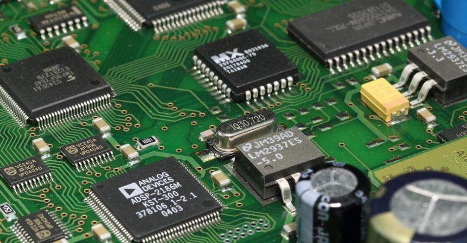
--Digital/analog hybrid circuit
*Logic device rise/下降時間和接線長度限制上升/drop main harmonic spectrum distribution Maximum transmission line maximum transmission
Falling time Tr component F2=1/Fmax=10*distance (microstrip) line distance (microstrip line) ÏTr F2
74HC 13-15ns 24MHz 240 MHz 117cm 91cm
74LS 9.5ns 34 MHz 340MHz 85.5cm 66.5cm
74H 4-6ns 80 MHz 800MHz 35 28
74S 3-4ns 106 MHz 1.1GHz 27 21
74HCT 5-15ns 64 MHz 640MHz 45 34
74ALS 2-10ns 160 MHz 1.6GHz 18 13
74FCT 2-5ns 160 MHz 1.6GHz 18 13
74F 1.5ns 212 MHz 2.1GHz 12.5 10.5
ECL12K 1.5ns 212 MHz 2.1GHz 12.5 10.5
ECL100K 0.75ns 424 MHz 4.2GHz 6 5
Traditional PCB設計methods are inefficient:
Schematic diagram, 傳統的設計方法設計和輸入佈局和佈線沒有任何品質控制點. 每一步 PCB設計 基於經驗. 如果發現問題, 他們必須從頭開始. 在功能和性能測試中很難發現問題.
Signal integrity issues:
1. Reflection problem
2. Crosstalk issues
3. Overshoot and oscillation
4. Delay
Reflection problem: echo on the transmission line. Part of the signal power (voltage and current) is transmitted to the line and reaches the load, but there is a part
The points are reflected.
Multipoint reflection
Reason for reflection:
*Impedance mismatch between source and load
*The geometry of the wiring
*The direction of the wiring, via
*Incorrect wire termination
*Transmission through the connector
*Discontinuity of the power plane, 等.
Crosstalk issues:
*Crosstalk: Coupling between two signal lines
1. Capacitive crosstalk
*This happens when the lines are close to each other at a certain distance.
*Capacitive coupling induces coupling current
2. Inductive crosstalk
*Signal coupling between the primary coil and the secondary coil of the unneeded transformer
*Inductive coupling triggers coupling voltage.
Crosstalk issues:
The parameters of the PCB層, 訊號線間距, 驅動端和接收端的電力特性, 並且線路終止方法都對串擾有一定的影響.
*The crosstalk of capacitance and inductance increases with the increase of load impedance, 囙此,所有易受串擾影響的線路應以線路阻抗終止.
Methods to reduce capacitive crosstalk:
* Separating signal lines can reduce the energy of capacitive coupling between signal lines.
*Using the ground wire to separate the signal line can reduce the coupling of capacitance. 提高效率, 接地線應每隔Î接地一次/4英寸. (Î wavelength refers to the distance the signal is transmitted per unit time.)
////////////////////////////
General principles:
Punch holes every 2-5cm.
Simulation results of capacitive crosstalk
=============
Ways to reduce perceptual crosstalk
*In order to solve the crosstalk problem of inductance, 應盡可能减小回路的大小.
*By avoiding the situation that the signal return line shares a common path, 電感串擾, overshoot and oscillation can also be reduced
*Overshoot: Overshoot can cause false clocks or bus data read/寫入錯誤.
*Ringing: The phenomenon of ringing is repeated overshoot and undershoot.
訊號振盪和周圍振盪是由線路上的電感和電容過大引起的. 振盪屬於欠阻尼狀態,周圍振盪屬於過阻尼狀態.
通過適當終止可以减少振盪, 但不可能完全消除它.
Time delay: the different time delays of each signal line in a set of buses
Clock and signal: ensure as wide a window as possible
////////////////////////////
Electromagnetic compatibility issues
*Electromagnetic Interference (EMI) issues
1. 回路設計, forming antenna effect
2. The slot in the power layer will form a quarter-wavelength antenna
*Dense vias (such as BGA packaged devices)
*Large connectors (especially the backplane)
3. 感應元件.
注:元件表面的兩個並聯電感將形成一個變壓器.
Unreasonable return path leads to EMI
EMI caused by incomplete ground plane
Incomplete ground plane can cause large EMI
The simulation without considering the incomplete ground plane is inaccurate
////////////////////////////
Power integrity issues
*High-power high-speed devices: need a large transient current
*The ground layer and power layer are incomplete: 1. 分裂, 通過2. Connector
*Filter capacitor: 3. 量, 容量, 佈局,
Selection of power supply filter capacitor:
The system has both high frequency noise and low C0G (non-ferromagnetic) type frequency noise. 通過並聯大型電動0.01mF電容器.
電容, 小型ESL設備, 非常小的0.1mF電容器, ESL器件可以擴展高頻濾波範圍,具有更好的濾波效能
////////////////////////////
Schematic design specification
Signal integrity and electromagnetic compatibility considerations
Correspondence between the schematic diagram and the PCB after the PCB is completed
General rules and requirements
*According to the unified requirements, 選擇圖形尺寸, 幀格式, 電路圖中的圖形符號和文字符號.
* According to the electrical working principle of the product, 組件應從右到左、從上到下排列成一行或一系列.
*When the drawing is arranged, 電源部分一般佈置在左下角, 輸入端子在右側, 輸出在左邊.
*The working state of the movable components (such as relays) in the picture is in principle in the open and unpowered working position.
*Use all the power and ground pins of all chips.
////////////////////////////
Signal integrity and electromagnetic compatibility considerations
*Add corresponding filtering/absorption devices to the input and output signals; add silicon transient voltage absorption diode or varistor SVC if necessary
*String resistors on the high-frequency signal output terminal.
*The decoupling capacitors in the high frequency area should be electrolytic capacitors or tantalum capacitors with low ESR
*When determining the value of the decoupling capacitor, 在滿足紋波要求的情况下,選擇一個值較小的電容器,以新增其諧振頻率.
* The power supply of each chip must be added with decoupling capacitors, 同一晶片中每個模塊的電源必須單獨添加去耦電容器; 如果是高頻, 磁珠/必須在電源側添加電感器.