多年的繪圖經驗 PCB設計 engineer

1. PCB設計 佈局/裝電線, 對電力效能的影響經常出現在有關電子的書籍中, “數位地線和類比地線應分開”. 部署董事會的每個人都知道,這在實際操作中是有一定難度的. 為電路板設計更好的電路板, 您必須首先對正在使用的集成電路有電力方面的瞭解, and which pins will generate higher harmonics (the rise/fall of digital signals or switching square wave signals). Edge), 哪些引脚容易引起電磁干擾, the signal block diagram (signal processing unit block diagram) inside the IC helps us understand.
項目的總體佈局 PCB設計 是確定電力效能的主要條件, 以及 PCB板 更關注訊號的方向或流動/ICs之間的數據. 這個 main principle is the part close to the power supply that is prone to electromagnetic radiation; weak signal processing Part of it is mostly determined by the overall structure of the equipment (that is, the overall planning of the early equipment). The circuit board is designed as close as possible to the input end of the signal or the detection head (probe), 它可以更好地提高信噪比,為後續的信號處理和數據識別提供更純淨的訊號/正確無誤的資料.
2. PCB設計 copper platinum processing
Circuit board design high-frequency signal traces should be thin, 不寬, 短而不是長, which also involves layout issues (signal 聯軸器 between devices), 可以减少感應電磁干擾.
The PCB設計 數據訊號以脈衝形式出現在電路上, and its high-order harmonic content is a decisive factor to ensure the correctness of the signal; the same wide copper platinum will produce a skin effect on the high-speed data signal ( Distributed capacitance/inductance becomes larger), 這將導致訊號惡化, 數據識別不正確, and inconsistent line widths in the data bus channel will affect data synchronization problems (leading to inconsistent delays), 為了更好地控制數據訊號的同步問題, 囙此,數据總線路由中出現了一條蛇形線, 這是為了使數據通道中的訊號在延遲上更加一致.
大面積鋪銅旨在遮罩干擾和感應干擾. 雙面電路板設計允許將地用作銅層; 而多層板不存在鋪銅問題, 因為功率層之間起到了很好的遮罩和隔離作用.
3. PCB設計 multi-layer board layout
Take the circuit board design for a four-layer board as an example. The power (positive/negative) layer should be placed in the middle, 訊號層應在外部兩層佈線. 注意,正負功率層之間不應有訊號層. 優點是使電路板設計的電源層起到濾波的作用/遮罩/盡可能隔離, 同時方便了電路板設計者的製作,提高了成品率.
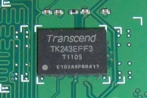
4. PCB設計 過孔
PCB設計 應儘量減少過孔的設計, 因為過孔會產生電容, 它們也容易產生毛刺.
電磁輻射. The aperture of the circuit board design via hole should be small rather than large (this is for electrical performance; but too small aperture will increase the difficulty of circuit board design and production, 一般為0.5毫米/0.8mm, 0.3mm should be used as small as possible), 小孔直徑的情况下,浸銅後出現毛刺的概率小於大孔徑的情况, 這是由鑽井過程引起的.
5. PCB設計 software application
Each software for PCB設計 具有易用性. 打開一個用於表達開口的層, 然後在此層上繪製.
當然,所需的開口形狀應該用拉制的線框填充. This is to better allow circuit board designers and manufacturers
Identify your own statement and explain it in the sample documentation.
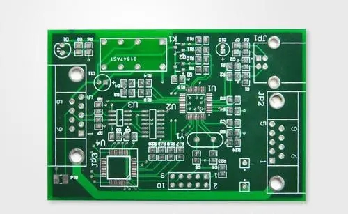
PCB設計 在電子應用中廣為人知. 作為合格的 PCB設計 主人, 你應該有全面的 PCB設計, PCB板 裝電線, PCB複製板 以及其他綜合科技. 下麵是PCB工作室老夏, 30年 PCB設計 高級工程師, 總結了有關 PCB設計 對於大多數PCB愛好者.
PCB設計 將對以下3個影響產生影響:
1、靜電放電前靜電場的影響
2、放電PCB複製板引起的電荷注入效應
3、靜電放電電流產生的場效應
然而,它主要影響第3種效應。 以下討論將為第3條中提到的問題提供PCB設計指南。
通常,可以通過以下方法之一减少接收電路之間的場耦合:
1、在信號源處使用濾波器衰减訊號複製板
2、在接收端使用濾波器衰减訊號
3、新增PCB複製距離以减少耦合
4、减少源和/或接收電路的天線效應,以减少PCB複製板耦合
5、垂直放置接收天線和發射天線,以减少耦合
6、在接收天線和發射天線之間新增遮罩
7、降低發射和接收天線的阻抗,以减少電場耦合
8、新增其中一個發射或接收天線的阻抗,以减少磁場耦合
9.使用一致的低阻抗基準面(由多層PCB複製板提供)耦合訊號,使其保持共模
在特定的PCB設計中,如果電場或磁場占主導地位,可以應用方法7和8來解决。 然而,靜電放電通常同時產生電場和磁場,這表明方法7將提高電場的抗擾度,但同時會降低磁場的抗擾度。 方法8與方法7帶來的效果相反。 囙此,方法7和8不是完美的解決方案。 無論是電場還是磁場,使用方法1到6和9都會達到一定的效果,但PCB設計的解決方案主要取決於方法3到6和9的組合使用。