1 這個 PCB資料 currently used by MITAC
A. Urea cardboard
Features: The color is light yellow, 通常用於單面面板, 但因為它是由尿素紙製成的, 在凉爽潮濕的地方很容易腐爛, 所以現在不常用.
B. CAM-3 board
Features: The color is milky white, 韌性好, it has a high CTI (600V), 二氧化碳排放量只有正常水准的四分之一. 它現在更常用於單面面板.
C. FR4. fiberboard
Characteristics: It is made of fiber, 具有良好的韌性, 當它破裂時, 電線互相拉著. 它通常用於多個面板. Its thermal expansion coefficient is 13 (16ppm/c). 我們廠用的主機板就是用這塊板做的.
D. Multilayer board
Features: high Tg, 高耐熱性和低熱膨脹率, 低介電常數和介質損耗資料, 主要用於四層或四層以上.
E. Soft board
Features: The 材料 is soft and transparent, 它通常用於兩塊板的電力連接, 而且很容易折疊. 例如, 筆記型電腦中LCD和機身之間的連接.

F. Other
With a personal computer. 隨著手機等多媒體數位資訊終端產品的普及, PCBA變得更輕, 更薄的, 更短的, 和更小. 國外一些大型集團公司相繼發展壯大 PCB板, 例如無鹵素, 無銻環保產品, 高耐熱性, 高Tg板, 熱膨脹係數低, 低介電常數, 和低介質損耗板. 其代表產品為:FR-5, Tg200板, 小便板, PI板, CEL-475, 等. 只是它在中國還不流行.
2. The current MITAC PCB-Layout 過程
Aï¹ R&D provides SCHMATIC (EE), FAB OUTLINE (ME) product development department provides us with schematic diagrams, 機械工程師為我們提供週邊資訊.
Bï¹ Create new part
We call out the part from LIBRARIAN accord在裡面g to the schematic diagram. 如果圖書管理員中沒有這樣的角色, 我們將創建一個新零件.
Cï¹ Part layout
After the parts are ready, we need to lay out the parts
Dï¹ ROUTING
This is our main task. 在我們安排好比賽之後, 我們將繼續路由.
Eï¹ Final finishing
After ROUTING, we need to use FABLINK to finally sort out the various data we need
Fï¹ Convert GERBER
Converted into GERBER documents required by PC board manufacturers
Gï¹ Data save
After all the work is done, save the data for later modification and verification
three. Some basic terms about printing plates
On an insulating base 材料, 根據預定設計, 印刷電路, 製作由二者組合形成的印刷元件或導電圖案, 這被稱為印刷電路. 在絕緣基板上, 在組件之間提供電力連接的導電圖案稱為印刷電路. 它不包括列印組件. 印刷電路或印刷電路的成品板稱為印刷電路板或印刷電路板, 也稱為印製板. 根據所用基材是剛性還是柔性,印製板可分為兩類:剛性印製板刷和柔性印製板. 今年也出現了剛柔印制板. 根據導體圖案的層數, 它們可以分為單面, 雙面和多層印製板. 導體圖案的整個外表面與基板表面在同一平面上. 該印版稱為平面印版.
電子設備採用印製板後,由於類似印製板的一致性,可以避免手動佈線錯誤,電子元件可以自動插入或安裝、自動焊接和自動檢測,確保電子設備的質量並提高其勞動生產率,降低成本,且易於維護。 印製板已從單層發展到雙面、多層和柔性,並仍保持各自的發展趨勢。 由於高精度、高密度和高可靠性的不斷發展方向,體積的不斷减小和成本的降低,使得印製板在未來的電子設備發展中仍保持著强大的生命力。
4. V-1 FR-4級?
FR-4(阻燃層壓板)是以“玻璃纖維布”為主體,浸漬液態阻燃“環氧樹脂”作為粘合劑形成薄膜,然後層壓形成各種厚度的板材。 所謂V-1是指寬度為0.5英寸、長度為5英寸和任意厚度的無銅玻璃纖維環氧樹脂基材的樣品。 量測火焰持續的秒數,等待火焰完全熄滅後再繼續燃燒。 連續十次試射後,總延遲小於250秒的被稱為V-1級FR-4,小於50秒的被稱為V-0級FR-4。
5. A brief history of PCB development
The basic concepts of printed circuits have been proposed in patents at the beginning of this century. 1947年, 美國航空管理局和美國標準局發起了第一次印刷電路技術研討會. 當時, 列出了26種不同的印刷電路製造方法. 它分為六類:塗層法, 噴塗方法, 化學沉積法, 真空蒸發法, 成型法和粉末壓實法. 當時, 這些方法未能實現大規模工業生產. 壓力板的粘附問題已得到解决, 覆銅板的效能穩定可靠, 實現了大規模工業化生產. 銅箔蝕刻法已成為印製板製造技術的主流,並發展到今天. 20世紀60年代, 孔金屬化雙面印刷和多層印製板已實現批量生產. 由於20世紀70年代大規模集成電路和電子計算器的快速發展, 隨著電路板生產科技的不斷進步,20世紀80年代表面貼裝科技和90年代多晶片組裝科技的快速發展促進了印刷業的發展, 許多新材料, 新設備, 新的測試儀器層出不窮. 印刷電路生產科技進一步向高密度方向發展, 細導線, 多層, 高可靠性, 低成本, 自動化連續生產. ï¹
6. Schematic design process
The generation of schematic diagram is generally regarded as the first step in the PCB production process. 它也是電子工程技術人員對產品視覺的具體實現. ) Is composed of different logical connections. 製作示意圖, the source of its logical components is that some CAD software contains a huge logical component library (such as TANGO PADS, 等.), and some CAD software is in addition to logic
In addition to the library of logical components, users can also add new logical components (such as Cadence, 導師, 祖肯, 等.) by themselves, 用戶可以使用這些邏輯組件來實現要設計的產品的邏輯功能.
1 Establish logic components
Logic components are components that provide a logic function (such as an LSOO gate, a flip-flop or an ASIC circuit).
1) The definition of the logical component model (or component name).
2) Package form of logic component pins
3) Description of logic component pins
4) Definition of the shape and symbol size of logical components
2 Functional description of logic components
To simulate the logic circuit, 有必要描述每個邏輯組件的功能特性, 例如邏輯元件的時序關係, the initial state rising edge (RISE), falling edge (FALL), 延遲時間, 和驅動衰减. 衰减時間, 等.
3 Description of the logic component library
Since there are many logic components, 它們建在一個圖書館下, 這很容易引起混亂,也很難管理. 因此, 具有類似功能特性的邏輯元件通常放在一個庫中,並根據功能特性進行管理, 例如/D, D/A轉換設備, CMOS器件, 儲存設備, TTL設備, 線性器件, 運算放大器設備, 比較設備, 等., 都放在同一個庫中. 它也可以由公司製造商進行分類,例如:摩托羅拉, NEC公司, 英特爾, 等.
.
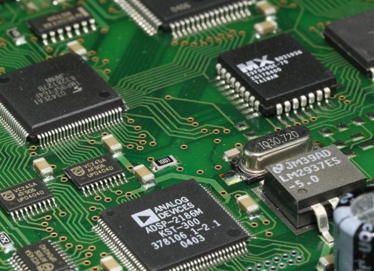
7. The function of printed circuit in electronic equipment
(1) Provide mechanical support for the fixing and assembly of various electronic components such as integrated circuits.
(2) Realize wiring and electrical connection or electrical insulation between various electronic components such as integrated circuits.
(3) Provide the required electrical characteristics, 例如特性阻抗, 等.
(4) Provide solder mask graphics for automatic soldering, 並為組件插入提供識別字和圖形, 視察, 和維護.
8. 為了滿足環境保護的要求, 將怎樣 PCB製造 科技變革?
1) Reduce lead content
The method of using electroplated lead-tin to make pattern plating is tending to be quickly abolished. 未來, there will be more conversion to the entire panel plating (Panel Plating, also known as: Panel Plating) process method. 在使用圖案電鍍生產方法的情况下, 電鍍錫也將成為主流. 如果使用焊料, 焊料將轉化為無鉛資料, 未來這一領域將取得更大進展. 預計這一變化對整個行業影響不大 PCB製造 process.
(2) Reduce the amount of formaldehyde used
Formaldehyde is used as a reducing agent for electroless copper plating (Electroless Copper Plating, 也稱為:化學鍍銅, electroless copper plating) in PCB production. 現時, 從環境保護的角度, 未來對其使用將有更嚴格的限制. 未來, 通過電鍍工藝的變化, 减少或消除甲醛資料的使用將是未來的發展趨勢. 直接電鍍將成為一種廣泛使用的電鍍方法. 重新認識使用這種電鍍方法的意義和進一步改進這一工藝是今後需要進行的重要任務.
(3) Progress of MID
Thermoplastic resin is a polymer 材料 that can be easily recycled. 為了滿足未來環境保護和生態環境維護的要求, 未來,熱塑性樹脂將更多地用於線路部件. It is called: Molded Interconnect Device (MID), 這將取代部分傳統的PCB製造技術. MID將成為PCB領域具有發展潜力的“新軍”.
(4) Other 材料
Solder resist 材料, printed circuit board substrate 材料 (flame-retardant non-halogen-containing base 材料) and other 材料 that are compatible with environmental protection will be developed and developed more and more quickly. 這也使得主要資料用於 PCB製造 流程變化很大. 因此, in PCB製造, the original process technology will be subject to considerable impact
9. High-speed circuit
It is generally believed that if the frequency of a digital logic circuit reaches or exceeds 45MHZ~50MHZ, and the circuit working above this frequency has taken up a certain share of the entire electronic system (for example, 1/3), 它被稱為高速電路.
n事實, 訊號邊緣的諧波頻率高於訊號本身的頻率. It is the rising and falling edges of the signal (or signal jump) that cause unexpected results of signal transmission. 因此, 一般認為,如果線路傳播延遲大於1/數位信號驅動端上升時間的2, 此類訊號被視為高速訊號,並產生傳輸線效應. 訊號傳輸發生在訊號狀態變化的瞬間, 例如上升或下降時間. 訊號從驅動端到接收端經過一段固定的時間. 如果傳輸時間小於1/上升或下降時間的2, 在訊號改變狀態之前,接收端的反射訊號將到達驅動端. 相反地, 訊號改變狀態後,反射訊號將到達驅動端. 如果反射訊號强, 疊加波形可能會改變邏輯狀態.
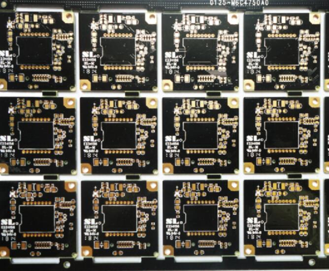
10.V_切割
One way to shape the circuit board is to cut straight lines at the same position on the upper and lower sides of the board without cutting, 囙此,可以手動或使用夾具從板的頂部和底部形成V形槽, so it is called V_CUT
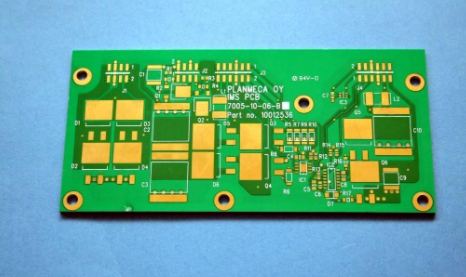
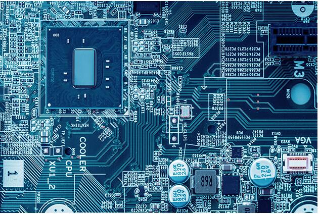
11 Golden finger
it refers to some PCB電路板 比如網卡. 上面板上的鍍金導線被稱為金手指,因為它們的形狀像手指.