iPCB有自己的 SMT晶片 工廠, 可以提供 SMT晶片 最小包裝中0201組件的處理服務, 並支持來料樣品和PCBA OEM資料的加工. 下一個, 我將介紹 SMT晶片 處理. 成本因素.
PCBA processing
Advantages of SMT加工
SMT processing is essentially the technology of soldering the components to the PCB light board through related machinery and equipment. 雖然機器的成本支出相對較大, 與傳統的挿件組裝相比,它有其獨特的優勢和特點. 這項科技有很多優點, 如整體PCBA處理效率和組件小型化. 以及成品體積的小型化. 因為這臺機器可以大批量生產, 這大大新增了勞動力相關限制導致的成本新增和效率低下, 這是整個電子製造業發展的科技陞級.
涉及的主要階段 SMT補丁處理 process
1. Solder paste printing
2. Solder paste inspection
3 Patch processing
4 Manual inspection
5 Reflow soldering
6 In (offline) AOI test
7 X-RAY detection
8 Functional test

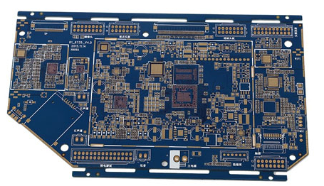
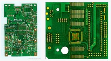
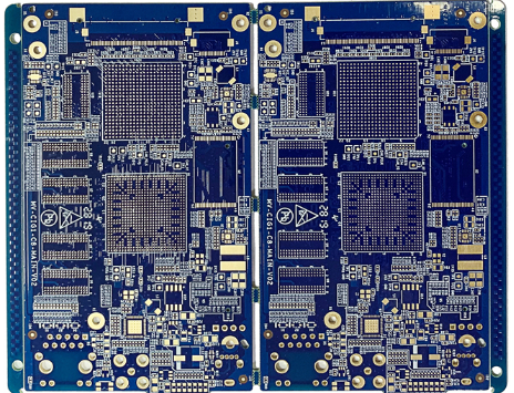
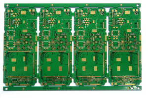
SMT processing factory
Factors affecting cost during SMT補丁處理
1. Solder Paste Printing
The process involves placing an accurate amount of solder paste on the pads of the components to be soldered. 出於這個原因, 錫膏的正確使用不僅重要, 但同樣重要的是,在低溫下妥善儲存,並在使用前恢復到室溫. 此外, 您還需要注意刮削角度和速度.
2. Solder paste inspection
This step is very helpful in reducing costs, 因為它有助於儘早發現SMT焊接缺陷. 它使您能够在製造的後期階段防止成本高昂的缺陷.
3. Patch processing
An important part of the SMT assembly process, 由貼片機完成. 雖然小型組件是通過高速貼片機安裝的, 大型組件需要低速運行的多功能貼片機.
4. Manual visual inspection
The visual inspection process once again ensures that any defects can be found early. 在此階段可以識別的一些錯誤包括任何缺失的零件或缺乏適當的放置. 回流焊後, 這些缺陷很難處理. 再一次, SMT組裝的這一階段允許成本控制, 好像這個階段還沒有實施, 您可以期望稍後更正錯誤,生產成本將上升.
5. Reflow soldering
This process involves melting the solder paste so that the component can be connected to the circuit board. 溫度分佈設定决定了再流焊能力,也降低了生產成本. 專業裝配工可以在很大程度上控制成本.
6. Automatic optical inspection
At this stage, 徹底檢查焊點的效能. Some errors that can be detected at this stage include:
Tombstone, 幾件, 混亂, 架橋, 虛擬焊接, 等.
7. X-ray detection
Once again, X射線檢查是一種很好的方法,可以確保產品的效率,並且在投放市場後不必與產品缺陷作鬥爭.
8. ICT or functional testing
Functional testing will continue to test the functions of the assembled PCB to ensure that the final product is very reliable.
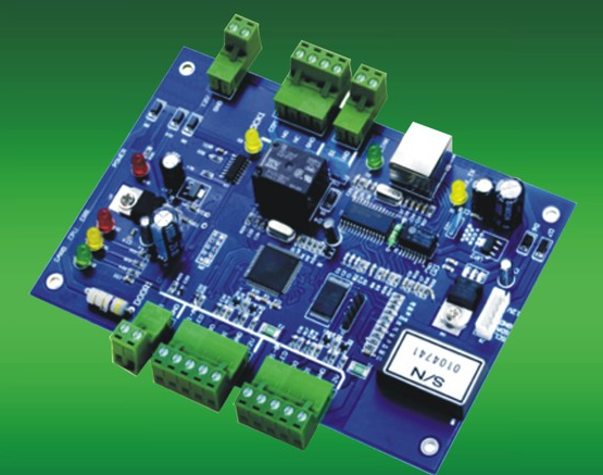
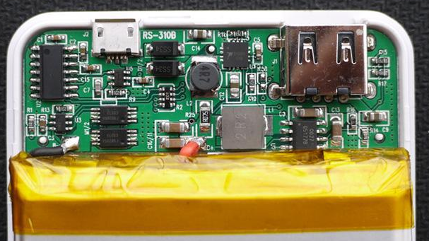
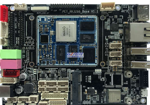
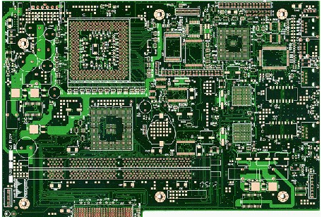
SMT processing
SMT晶片 processing capability
1. The largest board: 310mm*410mm (SMT);
2. Maximum board thickness: 3mm;
3. 最小板厚:0.5mm;
4. 最小晶片零件:0201封裝或0以上零件.6mm*0.3mm;
5. The maximum weight of mounted parts: 150 grams;
6. Maximum part height: 25mm;
7. Maximum part size: 150mm*150mm;
8. 最小引線零件間距:0.3mm;
9. The smallest spherical part (BGA公司) spacing: 0.3mm;
10. The smallest spherical part (BGA) diameter: 0.3mm;
11. Maximum component placement accuracy (100QFP): 25um@IPC;
12. 安裝容量:300萬到400萬點/白天.
為什麼選擇iPCB SMT補丁處理?
1. Strength guarantee
⪠SMT workshop: It has imported placement machines and multiple optical inspection equipment, 每天可以產生400萬個積分. 每道工序配備QC人員, 誰能關注產品品質.
–DIP生產線:有兩臺波峰焊機. 其中, 有十多比特工作了3年以上的老員工. 工人技術精湛,能焊接各種插入式資料.
2. 品質保證, high cost performance
⪠High-end equipment can paste precision shaped parts, BGA, QFN公司, 0201資料. 它也可用作手動安裝和放置散裝資料的模型.
–可以生產樣品和大小批量. 打樣起價800元, 批次從0開始.008元/指向, 而且沒有啟動費.
3. 有豐富的電子產品SMT和釺焊經驗, stable delivery
⪠Accumulated services to thousands of electronic companies, 涉及 SMT晶片 各類汽車設備和工業控制主機板加工服務. 產品經常出口到歐洲和美國, 質量得到新老客戶的肯定.
–按時交貨, 資料完成後的正常3-5天, 小批量也可以在同一天發貨.
4. Strong maintenance ability and perfect after-sales service
⪠The maintenance engineer has rich experience and can repair the defective products caused by all kinds of patch welding, 並能保證各電路板的連接率.
–24小時客服人員將隨時響應並儘快解決您的訂單問題.