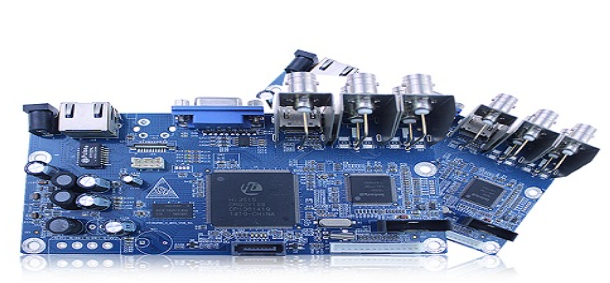
印刷電路板 過程 熱棒軟板 design can not be ignored
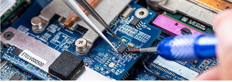
Hot-Bar reflow (melting tin hot pressure welding), its most important function is to use the hot press head to melt the solder paste that has been printed on the electronic printed circuit (印刷電路板), 以便連接兩個獨立的電子部件. The method is to solder the flexible flat cable (FPB) to the electronic printed circuit (印刷電路板).
由於熱棒機的熱壓頭是唯一的熱源, when the hot pressing head is pressed on the flexible flat cable (柔性線路板), 熱量必須向下傳遞到電子元件 印刷電路板(印刷電路板) to melt the printed circuit on the electronic printed circuit The solder paste on the board, 囙此,柔性扁平電纜必須具有導熱設計.
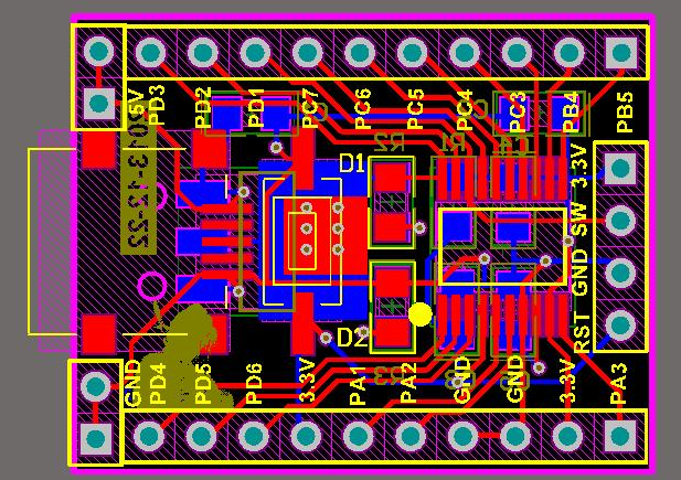
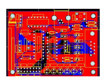
一般來說,在焊盤上製作電鍍孔或過孔是最常見的導熱功能設計,如下圖所示。 建議在每個柔性線路板的焊盤上有3個通孔或2.5個通孔。 製作電鍍孔還有一個優點。 在熔融錫的熱壓焊接操作過程中,多餘的錫可能會從電鍍孔溢出,從而不會導致焊盤之間短路。
柔性扁平電纜應貼上雙面膠帶,將柔性扁平電纜固定在電子印刷電路板上,因為操作員不太可能用手握住柔性線路板,直到熱棒回流完成。 此外,還可能出現質量不穩定的問題。
將柔性線路板的設計要求總結如下。 每個柔性線路板的焊盤上最好有3個電鍍孔或通孔,至少兩個+半電鍍孔或通孔。

Stick double-sided tape on the side of the flexible flat cable (FPB) that is attached to the electronic 印刷電路板. 雙面膠帶的厚度應小於0.15毫米, 以及與邊緣的距離 柔性線路板 雙面膠帶的襯墊應為0.20毫米. 距離.
推薦的 熱棒軟板 size design is as follows:
The aperture of the via hole is 0.4mm
Through hole center to center is 1.2mm
The distance from the center of the pad to the center is 1.8mm
The pad width is 0.9毫米
為了避免應力集中導致柔性扁平電纜斷裂,強烈建議錯開柔性扁平電纜的蓋膜(聚醯亞胺)邊緣。
為了配合熱棒操作,避免擠壓或損壞零件, the following is the recommended limit size of the parts:
The minimum dimension from the part to the front edge of the 柔性線路板 是2.0毫米.
零件到零件左右邊緣的最小尺寸 柔性線路板 是3.0毫米.
當 柔性線路板 向外延伸, 最小間距為5.應保留0mm,以便 柔性線路板 可以粘貼在 印刷電路板. 您也可以考慮在 柔性線路板, and designing alignment pins (Alignment Pins) on the hot press fixture for positioning, 這樣可以節省雙面膠帶和 印刷電路板, 但必須考慮準確性.
下零件的最小尺寸 柔性線路板 至 柔性線路板 是10.0mm (in order to ensure that the double-sided adhesive can be pasted on the 印刷電路板).