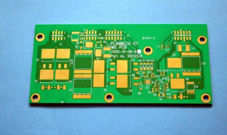
The PCB printed board design specifications of surface mount technology (SMT) and through-hole insertion technology (THT) are quite different. When determining the shape, land pattern and wiring method of the surface mount printed board, full consideration should be given to the type of PCB circuit board assembly, metodo di montaggio, placement accuracy, and soldering process. Solo in questo modo è possibile garantire la qualità della saldatura e migliorare l'affidabilità dei moduli funzionali.
1. Surface mount printed board shape and positioning design
The shape of the printed board must be processed by CNC milling. If calculated according to the placement machine accuracy ±0.02mm, the vertical parallel accuracy around the printed board, che è, the form and position tolerance should reach ±0.02mm.
For printed boards with an external dimension less than 50mm*50mm, è consigliabile adottare la forma di pannellatura. The specific size of the panel should be determined according to the specifications and specific requirements of the placement machine and screen printing machine.
La scheda stampata deve essere posizionata durante il processo di stampa mancante, and a positioning hole must be provided. Prendiamo come esempio la serigrafia DEK prodotta nel Regno Unito. La macchina è dotata di una coppia di perni di posizionamento D3mm. Correspondingly, almeno due fori di posizionamento D3mm devono essere impostati sui lati opposti o sulle linee diagonali del PCB, relying on the machine's vision system (Vision) and The positioning hole ensures the positioning accuracy of the printed board.
The circumference of the printed board should be designed with a process clamping edge whose width is generally (5±0.1) mm, e non ci dovrebbero essere modelli di terra e dispositivi nel bordo di serraggio del processo. If it is true that the board size is limited and the above requirements cannot be met, o il metodo di assemblaggio del pannello è adottato, the production method of adding a frame around the periphery can be adopted, lasciando il bordo di bloccaggio del processo, and manually breaking and removing the frame after the welding is completed.

2. The wiring method of the printed board
Try to go as short as possible, specialmente per circuiti a segnale ridotto. The shorter the line, minore è la resistenza e minore è l'interferenza. At the same time, la lunghezza della linea di accoppiamento deve essere il più breve possibile.
When changing the direction of the signal lines on the same layer, si dovrebbe evitare di girare ad angolo retto, and go diagonally as much as possible, e il raggio di curvatura dovrebbe essere più grande.
Trace width and center distance
The width of the printed board lines is required to be as consistent as possible, che favorisce la corrispondenza dell'impedenza. In terms of the printed board manufacturing process, la larghezza può essere 0.3mm, 0.2mm o anche 0.1mm, e la distanza del centro può anche essere 0.3mm, 0.2mm, 0.1mm. However, man mano che le linee diventano più sottili, the spacing becomes smaller, Nel processo produttivo, the quality will be more difficult to control, il tasso di rottami aumenterà, and the manufacturing cost will increase. A meno che l'utente non abbia requisiti particolari, the wiring principle of 0.Larghezza linea 3mm e 0.3mm line spacing is more appropriate, che può controllare efficacemente la qualità.
Design of power cord and ground wire
For power lines and ground lines, maggiore è l'area di cablaggio, the better, al fine di ridurre le interferenze. For high-frequency signal lines, è meglio proteggerli con fili di terra.
Multilayer board routing direction
The wiring of the multilayer board should be separated according to the power layer, strato di terra e strato di segnale per ridurre l'interferenza tra potenza, ground and signals. Il cablaggio di schede multistrato richiede che le linee di due strati adiacenti di schede stampate siano il più possibile perpendicolari l'una all'altra, or slanted or curved, e non parallelo, so as to help reduce the coupling and interference between the substrate layers. Lo strato di potenza di grande area e lo strato di terra di grande area dovrebbero essere adiacenti l'uno all'altro, e la sua funzione è quella di formare un condensatore tra l'alimentazione elettrica e il terreno per svolgere un ruolo filtrante.
3 Pad design control
Because there is no unified standard for surface mount components, diversi paesi e produttori diversi hanno forme e pacchetti diversi di componenti. Pertanto, when choosing the pad size, Deve essere coerente con la forma del pacchetto dei componenti che scegli. Compare the size of the pins and other related soldering to determine the length and width of the pad.
Land length
The length of the pad plays a more important role in the reliability of the solder joint than the width of the solder joint. L'affidabilità del giunto di saldatura dipende principalmente dalla lunghezza piuttosto che dalla larghezza. As shown in Figure 1.
Figure 1 Solder joint
The selection of L1 and L2 size should be conducive to the formation of a good meniscus profile when the solder is melted, and also to avoid the bridging phenomenon of the solder, and take into account the deviation of the components (the deviation is within the allowable range) to facilitate the increase Adhesion of solder joints improves soldering reliability. Generally, L1 richiede 0.5mm and L2 takes 0.5-1.5mm.
Land width
For RC components above 0805, or SD, SOJ, and other IC chips with a pin pitch above 1.27mm, the pad width is generally based on the component pin width plus a value, e l'intervallo di valori è 0.1- Tra 0.25mm. Per un chip IC pari a 0.65mm including a pin pitch of 0.65 mm o meno, the width of the pad should be equal to the width of the pin. Per QFP a passo fine, sometimes the pad width should be appropriately reduced relative to the pins, come quando c'è un cavo che passa tra i due pad.
Requirements for lines between pads
It is necessary to avoid crossing wires between pads of fine-pitch components as much as possible. Se è necessario incrociare i fili tra le pastiglie, solder masks should be used to reliably shield them.
Requirement of pad symmetry
For the same component, all pads used symmetrically, come QFP, SOIC, ecc., should be designed to strictly ensure their overall symmetry, che è, the shape and size of the pad pattern are exactly the same to ensure that the solder will act on the component when the solder melts. La protezione della tensione superficiale di tutti i giunti di saldatura del dispositivo è bilanciata per facilitare la formazione di giunti di saldatura ideali di alta qualità e garantire nessun spostamento.
4 Benchmark standard (Mark) design requirements
A fiducial mark must be set on the printed circuit board to serve as a reference point for the placement machine during placement operations. Diversi tipi di macchine di posizionamento hanno requisiti diversi per la forma e le dimensioni del punto di riferimento. Generally, 2-3 D1.5mm bare copper solids are set on the diagonal of the printed board as the reference mark.
Per componenti multi-pin, especially fine-pitch mounted ICs with a pin pitch below 0.65mm, a fiducial mark should be added near the pad pattern, e due punti fiduciali simmetrici dovrebbero essere impostati sulla diagonale del modello pad. The mark is used for the optical positioning and calibration of the placement machine.
5 Other requirements
Transition hole treatment
Transition holes are not allowed in the pad, and the filter hole should be avoided to connect with the pad to avoid poor soldering caused by the loss of solder. Se il foro di transizione deve essere collegato con il pad, and the distance between the transition hole and the edge of the pad is greater than 1mm.
Characters and graphics requirements
Symbols such as characters, graphics, ecc. non deve essere stampato sul pad per evitare una scarsa saldatura.
6 concluding remarks
As a surface mount printed circuit board design technician, oltre ad avere familiarità con le pertinenti conoscenze teoriche della progettazione del circuito, you must also understand the surface mount production process, Conoscere il profilo dei componenti packaging di varie aziende che vengono spesso utilizzate, and many soldering quality problems are related to Poor design is directly related. Secondo il concetto di controllo dell'intero processo di produzione, surface mount printed circuit board design is a key and important link to ensure the quality of the surface mount.
Quanto sopra è un'introduzione ai requisiti di progettazione delle schede stampate a montaggio superficiale. Ipcb also provides PCB manufacturers and PCB manufacturing technology.