1. Il Materiale PCB currently used by MITAC
A. Urea cardboard
Features: The color is light yellow, often used for single-sided panels, ma perché è fatto di carta urea, it is easy to rot in a cool and humid place, so it is not commonly used now.
B. CAM-3 board
Features: The color is milky white, the toughness is good, it has a high CTI (600V), e l'emissione di anidride carbonica è solo un quarto del normale. It is now more commonly used in single-sided panels.
C. FR4 fiberboard
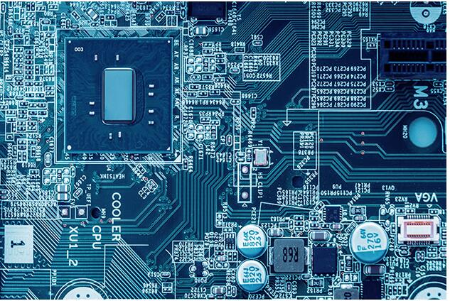
Characteristics: It is made of fiber, has good toughness, e quando si rompe, there are wires pulling each other. It is often used for multiple panels. Its thermal expansion coefficient is 13 (16ppm/c). The mother board used by our factory is made of this board.
D. Multilayer board
Features: high Tg, Elevata resistenza al calore e basso tasso di espansione termica, bassa costante dielettrica and dielectric loss materials, mostly used for four or more layers.
E. Soft board
Features: The material is soft and transparent, è spesso utilizzato nel collegamento elettrico di due schede, ed è facile da piegare. For example, la connessione tra l'LCD e il corpo del computer in un computer portatile.

F. Other
With a personal computer. With the popularity of multimedia digital information terminal products such as mobile phones, I PCB sono diventati più leggeri, thinner, più breve, and smaller. Alcune grandi società del gruppo all'estero si sono progressivamente sviluppate Schede PCB, such as halogen-free, prodotti ecologici privi di antimonio, high heat resistance, tavole ad alto Tg, low thermal expansion coefficient, low dielectric constant, and low dielectric loss boards. I suoi prodotti rappresentativi sono: FR-5, Tg200 board, Scheda PEE, PI board, CEL-475, ecc. It s just that it s not popular in China yet.
2. The current MITAC PCB-Layout process
Aï¹ R&D provides SCHMATIC (EE), FAB OUTLINE (ME) product development department provides us with schematic diagrams, and mechanical engineers provide us with peripheral information.
Bï¹ Create new part
We call out the part from LIBRARIAN according to the schematic diagram. If there is no such part in LIBRARIAN, creeremo una nuova parte.
Cï¹ Part layout
After the parts are ready, we need to lay out the parts
Dï¹ ROUTING
This is our main task. Dopo aver organizzato il gioco, we will proceed to ROUTING.
Eï¹ Final finishing
After ROUTING, we need to use FABLINK to finally sort out the various data we need
Fï¹ Convert GERBER
Converted into GERBER documents required by PC board manufacturers
Gï¹ Data save
After all the work is done, save the data for later modification and verification
three. Some basic terms about printing plates
On an insulating base material, secondo un progetto predeterminato, a printed circuit, un componente stampato o un modello conduttivo formato da una combinazione dei due sono realizzati, che è chiamato circuito stampato. On an insulating substrate, un modello conduttivo che fornisce collegamenti elettrici tra i componenti è chiamato circuito stampato. It does not include printing components. I pannelli finiti dei circuiti stampati o dei circuiti stampati sono chiamati circuiti stampati o circuiti stampati, also known as printed boards. I pannelli stampati possono essere suddivisi in due categorie a seconda che il substrato utilizzato sia rigido o flessibile: pennelli rigidi e pannelli stampati flessibili. Rigid-flexible printed boards have also appeared this year. Secondo il numero di strati di modelli conduttori, they can be divided into single-sided, schede stampate su due lati e multistrato. L'intera superficie esterna del modello conduttore è sullo stesso piano della superficie del substrato. Il piatto di stampa è chiamato un piatto di stampa piana.
Dopo che l'apparecchiatura elettronica adotta schede stampate, a causa della consistenza di schede stampate simili, gli errori di cablaggio manuali possono essere evitati e i componenti elettronici possono essere inseriti o montati automaticamente, saldatura automatica e rilevamento automatico, garantendo la qualità delle apparecchiature elettroniche e migliorando la produttività del lavoro, riduce i costi ed è facile da mantenere. Le schede di stampa si sono sviluppate da monostrato a bifacciale, multistrato e flessibili, mantenendo le rispettive tendenze di sviluppo. Grazie allo sviluppo continuo di alta precisione, alta densità e alta affidabilità Lo sviluppo della direzione, la riduzione continua del volume e la riduzione del costo, fanno sì che la scheda stampata mantenga ancora una forte vitalità nello sviluppo di apparecchiature elettroniche in futuro.
4. Grado V-1 FR-4?
FR-4 (flame-resistant laminated board) is based on "glass fiber cloth" as the main body, impregnato di "resina epossidica" liquida resistente alla fiamma come legante per formare un film, and then laminated to form boards of various thicknesses. Il cosiddetto V-1 si riferisce a un campione di un substrato di resina epossidica in fibra di vetro privo di rame con una larghezza di 0.5 inches, una lunghezza di 5 pollici e uno spessore arbitrario. Measure the number of seconds for the flame to continue, e attendere che la fiamma si spenga completamente prima di continuare a bruciare. After ten consecutive trial firings, quelli con un ritardo totale inferiore a 250 secondi sono chiamati V-1 grado FR-4, e quelli con meno di 50 secondi sono chiamati V-0 grado FR-4.
5. A brief history of PCB development
The basic concepts of printed circuits have been proposed in patents at the beginning of this century. In 1947, L'American Aviation Administration e l'American Bureau of Standards hanno avviato il primo seminario tecnico sui circuiti stampati. At that time, Sono stati elencati 26 diversi metodi di produzione dei circuiti stampati. È classificato in sei categorie: metodo di rivestimento, spraying method, metodo di deposizione chimica, vacuum evaporation method, metodo di stampaggio e compattazione delle polveri. At that time, questi metodi non sono riusciti a realizzare una produzione industriale su larga scala. The adhesion problem of the pressure plate has been solved, le prestazioni del laminato rivestito di rame sono stabili e affidabili, and large-scale industrial production has been realized. Il metodo di incisione del foglio di rame è diventato il mainstream della tecnologia di produzione del cartone stampato ed è stato sviluppato fino ad oggi. In the 1960s, La stampa di superficie e le schede stampate multistrato hanno raggiunto la produzione di massa. Due to the rapid development of large-scale integrated circuits and electronic calculators in the 1970s, Il rapido sviluppo della tecnologia di montaggio superficiale negli anni '80 e la tecnologia di assemblaggio multi-chip negli anni '90 ha promosso la stampa con il continuo progresso della tecnologia di produzione di circuiti stampati, a number of new materials, nuove attrezzature, and new testing instruments have emerged one after another. La tecnologia di produzione dei circuiti stampati si è ulteriormente sviluppata nella direzione dell'alta densità, thin wires, multistrato, high reliability, basso costo, and automated continuous production. ï¹
6. Schematic design process
The generation of schematic diagram is generally regarded as the first step in the PCB production process. It is also the specific realization of the product vision by electronic engineering and technical personnel. ) Is composed of different logical connections. To make a schematic diagram, the source of its logical components is that some CAD software contains a huge logical component library (such as TANGO PADS, ecc.), and some CAD software is in addition to logic
In addition to the library of logical components, users can also add new logical components (such as Cadence, Mentor, ZukenCity in Germany, etc.) by themselves, and users can use these logical components to implement the logical functions of the product to be designed.
1 Establish logic components
Logic components are components that provide a logic function (such as an LSOO gate, a flip-flop or an ASIC circuit).
1) The definition of the logical component model (or component name).
2) Package form of logic component pins
3) Description of logic component pins
4) Definition of the shape and symbol size of logical components
2 Functional description of logic components
To simulate the logic circuit, è necessario descrivere le caratteristiche funzionali di ogni componente logico, such as the timing relationship of the logic component, the initial state rising edge (RISE), falling edge (FALL), tempo di ritardo, and drive attenuation. Tempo di decadenza, etc.
3 Description of the logic component library
Since there are many logic components, they are built under one library, facile da creare confusione e difficile da gestire. Therefore, componenti logici con caratteristiche funzionali simili sono generalmente collocati sotto un'unica libreria e gestiti secondo caratteristiche funzionali, such as A/D, D/Un dispositivo di conversione , CMOS devices, dispositivi di memorizzazione, TTL devices, dispositivi lineari, op amp devices, dispositivi di confronto, etc., sono tutti collocati nella stessa libreria. It can also be classified by company manufacturers such as: MOTOROLA, NEC, INTEL, etc.
.
7. The function of printed circuit in electronic equipment
(1) Provide mechanical support for the fixing and assembly of various electronic components such as integrated circuits.
(2) Realize wiring and electrical connection or electrical insulation between various electronic components such as integrated circuits.
(3) Provide the required electrical characteristics, come impedenza caratteristica, etc.
(4) Provide solder mask graphics for automatic soldering, and provide identifiers and graphics for component insertion, ispezione, and maintenance.
8. In order to meet the requirements of environmental protection, how will PCB manufacturing technology change?
1) Reduce lead content
The method of using electroplated lead-tin to make pattern plating is tending to be quickly abolished. In futuro, there will be more conversion to the entire panel plating (Panel Plating, also known as: Panel Plating) process method. In the case of using pattern electroplating production method, La galvanizzazione dello stagno diventerà anche il mainstream. In the case of using solder, la saldatura sarà convertita in materiale privo di piombo, and there will be greater progress in this area in the future. Si prevede che questo cambiamento avrà un impatto limitato sull'intero processo di produzione dei PCB.
(2) Reduce the amount of formaldehyde used
Formaldehyde is used as a reducing agent for electroless copper plating (Electroless Copper Plating, noto anche come: placcatura di rame elettroless, electroless copper plating) in PCB production. Attualmente, from the perspective of environmental protection, ci saranno restrizioni più severe al suo utilizzo in futuro. In the future, attraverso cambiamenti nel processo di galvanizzazione, Ridurre o eliminare l'uso di materiali formaldeide sarà il trend di sviluppo futuro. Direct electroplating will become a widely used electroplating method. La ri-comprensione dell'importanza dell'uso di questo metodo di galvanizzazione e l'ulteriore miglioramento di questo processo sono compiti importanti che devono essere svolti in futuro.
(3) Progress of MID
Thermoplastic resin is a polymer material that can be easily recycled. Per soddisfare i requisiti di protezione ambientale e mantenimento dell'ambiente ecologico in futuro, thermoplastic resins will be used more in line circuit parts in the future. It is called: Molded Interconnect Device (MID), which will replace part of the traditional manufacturing technology PCB. MID diventerà un "nuovo esercito" con potenziale di sviluppo in PCB.
(4) Other materials
Solder resist materials, printed circuit board substrate materials (flame-retardant non-halogen-containing base materials) and other materials that are compatible with environmental protection will be developed and developed more and more quickly. This also makes the main materials used in the PCB manufacturing process change greatly. For this reason, nella produzione di PCB, the original process technology will be subject to considerable impact
9. High-speed circuit
It is generally believed that if the frequency of a digital logic circuit reaches or exceeds 45MHZ~50MHZ, and the circuit working above this frequency has taken up a certain share of the entire electronic system (for example, 1/3), it is called a high-speed circuit.
n fatto, the harmonic frequency of the signal edge is higher than the frequency of the signal itself. It is the rising and falling edges of the signal (or signal jump) that cause unexpected results of signal transmission. Therefore, è generalmente convenuto che se il ritardo di propagazione della linea è superiore a 1/2 of the rise time of the digital signal driving end, tali segnali sono considerati segnali ad alta velocità e producono effetti sulla linea di trasmissione. The transmission of the signal occurs at the instant when the signal state changes, such as the rise or fall time. Il segnale passa un periodo di tempo fisso dall'estremità di guida all'estremità di ricezione. If the transmission time is less than 1/2 of the rising or falling time, il segnale riflesso dall'estremità ricevente raggiungerà l'estremità di guida prima che il segnale cambi stato. Conversely, the reflected signal will reach the drive end after the signal changes state. If the reflected signal is strong, la forma d'onda sovrapposta può cambiare lo stato logico.
10. V_CUT
One way to shape the circuit board is to cut straight lines at the same position on the upper and lower sides of the board without cutting, so that it can be broken manually or using a jig to form a V-shaped groove from the top and bottom of the board, so it is called V_CUT
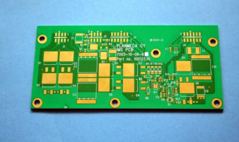
11.. Golden finger
it refers to some PCB circuit boards such as network cards. I fili dorati sul pannello superiore sono chiamati dita dorate perché sono a forma di dita.