ipcb è specializzata nella fornitura di servizi globali di produzione elettronica PCB, including one-stop services from upstream electronic component procurement to PCB production and processing, Patch SMT, DIP plug-in, Prova PCB, and finished product assembly. Avanti, I will introduce the common causes of welding defects in PCB processing.
Elaborazione PCBmanufacturers
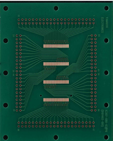
Analysis of the Causes of PCB Processing Welding Defects
1. The weldability of the board hole affects the welding quality
The poor solderability of the circuit board holes will result in Elaborazione PCBe difetti di saldatura, which will affect the parameters of the components in the circuit, con conseguente conduzione instabile tra i componenti della scheda multistrato e la linea interna, resulting in the failure of the entire circuit. La cosiddetta saldabilità si riferisce alla proprietà che la superficie metallica è bagnata da saldature fuse, that is, a relativamente uniforme, continuous and smooth adhesion film is formed on the metal surface of the solder.
I principali fattori che influenzano la saldabilità di circuiti stampati:
(1) The composition of the solder and the properties of the solder. La saldatura è una parte importante del processo di trattamento chimico della saldatura. It is composed of chemicals containing flux. I metalli eutettici a basso punto di fusione comunemente usati sono Sn-Pb o Sn-Pb-ag. The impurity content should be controlled in a certain proportion. Per evitare che gli ossidi generati dalle impurità vengano dissolti dal flusso. The function of the flux is to help the solder to wet the surface of the soldered board by transferring heat and removing rust. Solventi a colofonia bianca e isopropanolo sono generalmente utilizzati.

(2) The welding temperature and the cleanliness of the metal plate surface also affect the weldability. When the temperature is too high, aumenta la velocità di diffusione della saldatura. At this time, l'attività è elevata, the circuit board and the melting surface of the solder are rapidly oxidized, causare difetti di saldatura, and the surface of the circuit board is contaminated, che influisce anche sulla saldabilità e causa difetti. Including tin beads, palline di latta, disconnection, scarsa lucentezza, etc.
2. Elaborazione PCBwelding defects caused by warpage
Circuit boards and components warp during welding, e cause di deformazione da stress Elaborazione PCBwelding defects such as solder joints and short circuits. La guerra è spesso causata dallo squilibrio di temperatura tra la parte superiore e inferiore della scheda. For large PCBs, La deformazione può verificarsi a causa del peso della scheda stessa. Ordinary PBGA devices are about 0.5 mm di distanza dal circuito stampato. If the equipment on the circuit board is large, il circuito stampato tornerà alla sua forma normale dopo il raffreddamento, and the solder joints will be stressed for a long time.
3. PCB design affects welding quality
In the PCB design layout, quando la dimensione del circuito stampato è troppo grande, although the soldering is easier to control, ma la linea stampata è lunga, l'impedenza aumenta, the noise resistance decreases, e gli aumenti dei costi. String. Interferenza reciproca, such as electromagnetic interference to the board.
Pertanto, the PCB design must be optimized:
(1) Shorten the wiring between high-frequency components to reduce electromagnetic interference.
(2) Parts with heavier weight (such as 20g or more) are fixed with brackets and then welded.
(3) Heat dissipation issues should be considered for heating elements to prevent large defects and rework on the surface of the elements. Gli elementi termici devono essere tenuti lontani dalle fonti di calore.
(4) The arrangement of the components is as parallel as possible, che è bello e facile da saldare, and should be mass-produced. La scheda è progettata come il miglior rettangolo 4:3. Do not change the line width to avoid intermittent wiring. Quando la tavola è riscaldata per molto tempo, the copper foil is easy to swell and fall off, in modo da evitare fogli di rame di grande area.
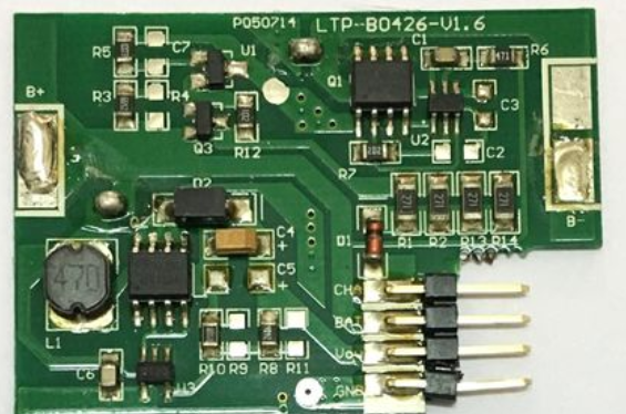
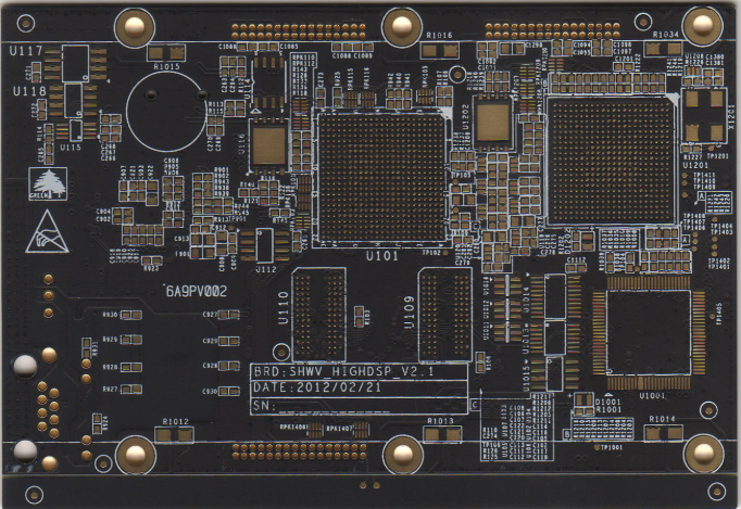
SMT factory explains the circuit board processing process in detail
Elaborazione PCBcapability
1. The largest board: 310mm*410mm (SMT);
2. Maximum board thickness: 3mm;
3. Minimum board thickness: 0.5mm;
4. The smallest Chip parts: 0201 package or parts above 0.6mm*0.3mm;
5. The maximum weight of mounted parts: 150 grams;
6. Maximum part height: 25mm;
7. Maximum part size: 150mm*150mm;
8. Distanza minima delle parti in piombo: 0.3mm;
9. The smallest spherical part (BGA) spacing: 0.3mm;
10. The smallest spherical part (BGA) diameter: 0.3mm;
11. Maximum component placement accuracy (100QFP): 25um IPC;
12. Mounting capacity: 3 to 4 million points/giorno.
PCB processing
Why chooseipcb?
1. Strength guarantee
ªSMT workshop: It has imported placement machines and multiple optical inspection equipment, che può produrre 4 milioni di punti al giorno. Each process is equipped with QC personnel, che possono tenere d'occhio la qualità del prodotto.
ªDIP production line: There are two wave soldering machines. Tra loro, there are more than ten old employees who have worked for more than three years. I lavoratori sono altamente qualificati e possono saldare tutti i tipi di materiali plug-in.
2. Garanzia della qualità, high cost performance
ªHigh-end equipment can paste precision shaped parts, BGA, QFN, 0201 materiali. It can also be used as a model for mounting and placing bulk materials by hand.
3. Rich experience in SMT and soldering of electronic products, stable delivery
ªAccumulated services to thousands of electronic companies, involving SMT chip processing services for various types of automotive equipment and industrial control motherboards. I prodotti vengono spesso esportati in Europa e negli Stati Uniti, e la qualità può essere affermata da nuovi e vecchi clienti.
ªDelivery on time, normale 3-5 giorni dopo che i materiali sono completi, and small batches can also be shipped on the same day.
4. Strong maintenance ability and perfect after-sales service
ªThe maintenance engineer has rich experience and can repair the defective products caused by all kinds of patch welding, and can ensure the connection rate of each circuit board.
ª24-hour customer service staff will respond at any time and solve your order problems as quickly as possible.