Metodo di placcatura PCB
One, brush plating
It is an electrodeposition technique, in which not all parts are immersed in the electrolyte during the electroplating process. In this electroplating technique, only a limited area is electroplated, and there is no effect on the rest.
Usually, rare metals are plated on selected parts of the printed circuit board, such as the edge of the board connector. Brush plating is used more when repairing discarded circuit boards in the electronic assembly workshop. A special anode (chemical The reactively inactive anode, such as graphite, is wrapped in an absorbent material (cotton swab) and used to bring the electroplating solution to the place where electroplating is required.
Secondo, placcatura a foro passante
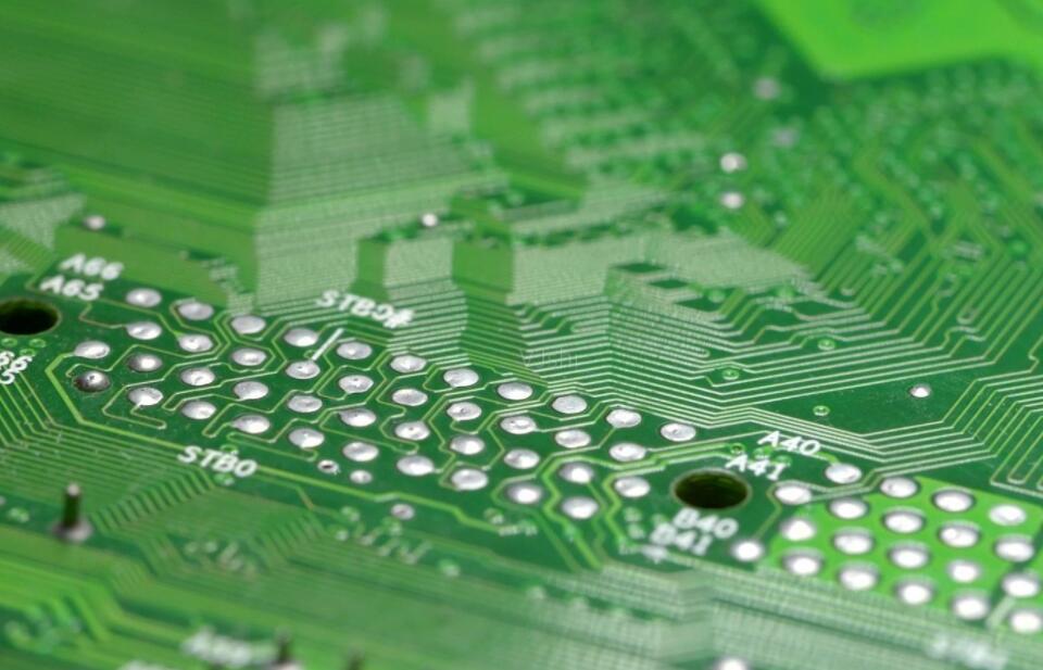
In through-hole plating, there are many ways to build a layer of electroplating layer on the hole wall of the substrate drilled hole, which is called hole wall activation in industrial applications. The commercial production process of its printed circuit requires multiple intermediate storage Tank, each storage tank has its own control and maintenance requirements.

Through hole plating is a necessary follow-up process of the drilling process. When the drill bit drills through the copper foil and the substrate below, the heat generated melts the insulating synthetic resin that constitutes most of the substrate matrix, the molten resin and other drilling debris It is piled up around the hole and coated on the newly exposed hole wall in the copper foil.
Infatti, questo è dannoso per la successiva superficie galvanica. La resina fusa lascerà anche uno strato di albero caldo sulla parete del foro del substrato. Mostra scarsa adesione alla maggior parte degli attivatori, che richiede lo sviluppo di un'altra tecnologia A simile alla rimozione delle macchie e all'incisione chimica posteriore, inchiostro!
The ink is used to form a high-adhesion, high-conductivity film on the inner wall of each through hole, so that there is no need to use multiple chemical treatment processes, only one application step, and then heat curing, it can be on all the hole walls. The inner side forms a continuous film, which can be directly electroplated without further processing. This ink is a resin-based substance, which has strong adhesion and can be easily bonded to most hot-polished holes On the wall, this eliminates the step of etchback.
Tre, placcatura selettiva del tipo di collegamento della bobina
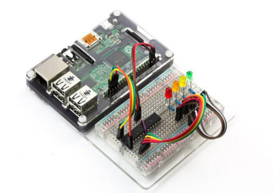
I perni e i perni dei componenti elettronici, quali connettori, circuiti integrati, transistor e circuiti stampati flessibili, sono tutti utilizzati placcatura selettiva per ottenere una buona resistenza al contatto e resistenza alla corrosione.
Questo metodo di galvanizzazione può utilizzare linee di produzione manuali di galvanizzazione o apparecchiature automatiche di galvanizzazione. È molto costoso selezionare ogni perno separatamente, quindi deve essere utilizzata la saldatura batch. Nella produzione di galvanizzazione, la lamina metallica viene solitamente laminata allo spessore richiesto. Le due estremità del tubo sono perforate, pulite con metodi chimici o meccanici e quindi utilizzate selettivamente per galvanizzazione continua come nichel, oro, argento, rodio, pulsante o lega di stagno-nichel, lega di rame-nichel, lega di nichel-piombo, ecc.
Quattro, attrezzatura di galvanizzazione di tipo di fila del dito
Nella galvanizzazione, è spesso necessario placcare metalli rari su connettori bordo bordo, contatti sporgenti bordo bordo bordo o dita dorate per fornire una minore resistenza al contatto e una maggiore resistenza all'usura. Questa tecnologia è chiamata placcatura di fila del dito o elettroplaccatura della parte sporgente. .
In electroplating, gold is often plated on the protruding contacts of the board edge connector with the inner plating layer of nickel. The gold fingers or the protruding parts of the board edge use manual or automatic electroplating technology. At present, the gold plating on the contact plug or gold finger has been plated. Lead, instead of plated buttons.
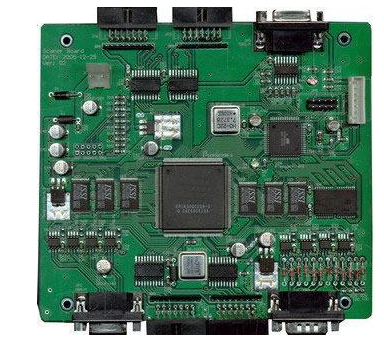
ipcb is a high-precision, high-quality PCB manufacturer, such as: isola 370hr PCB, high-frequency PCB, high-speed PCB, ic substrate, ic test board, impedance PCB, HDI PCB, Rigid-Flex PCB, buried blind PCB, advanced PCB, microwave PCB, telfon PCB and other ipcb are good at PCB manufacturing.